DESCRIPTION
¾ ¾ ¾ ¾ ¾ FEATURES
-30V/-4.9A, RDS(ON) = 65mΩ @ VGS = -10V -30V/-3.6A, RDS(ON) = 105mΩ @ VGS = -4.5V Super high dense cell trench design for low RDS(ON) Rugged and reliable SOP-8 package design ¾ ¾ ¾ ¾ APPLICATIONS
POWER Management in Note Portable Equipment Battery Powered System DC/DC Converter LCD Display ¾ PIN CONFIGURATION -1- Ver 1.01 6/2/2009. Datasheet pdf - MT4953 Dual P-Channel High Density Trench MOSFET ABSOLUTE MAXIMUM RATINGS
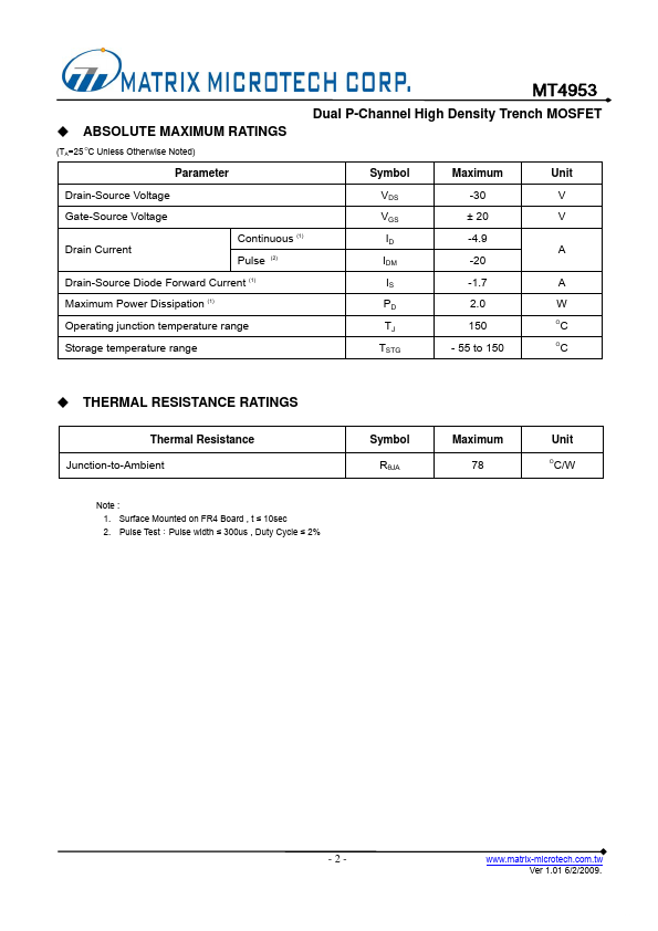
O (TA=25 C Unless Otherwise Noted) Parameter Drain-Source Voltage Gate-Source Voltage Drain Current Continuous (1) Pulse (2) Symbol VDS VGS ID IDM IS PD TJ TSTG Maximum -30 ± 20 -4.9 -20 -1.7 2.0 150 - 55 to 150 Unit V V A A W O Drain-Source Diode Forward Current (1) Maximum Power Dissipation (1) Operating junction temperature range Storage temperature range C C O THERMAL RESISTANCE RATINGS Thermal Resistance Symbol RθJA Maximum 78 Unit O Junction-to-Ambient C/W Note : 1. Surface Mounted on FR4 Board , t ≤ 10sec 2. Pulse Test:Pulse width ≤ 300us , Duty Cycle ≤ 2% -2- Ver 1.01 6/2/2009. matrix microtech