
MT28F400B3 Overview
Writing or erasing the device is done with either a 3.3V or 5V VPP voltage, while all operations are performed with a 3.3V VCC. Due to process technology advances, 5V VPP is optimal for application and production programming. These devices are fabricated with Micron’s advanced 0.18µm CMOS floating-gate process.
MT28F400B3 Key Features
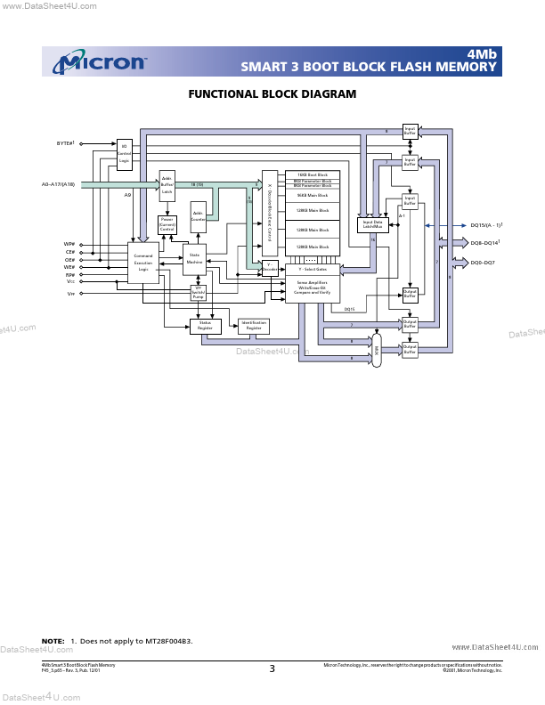
- Seven erase blocks: 40-Pin 16KB/8K-word boot block (protected) Two 8KB/4K-word parameter blocks Four main memory blocks
- patible with 0.3µm Smart 3 device
- Advanced 0.18µm CMOS floating-gate process
- Address access time: 80ns
- 100,000 ERASE cycles
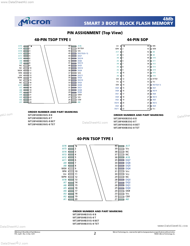
- Industry-standard pinouts
- Inputs and outputs are fully TTL-patible
- Automated write and erase algorithm
- Two-cycle WRITE/ERASE sequence
- Byte-wide READ and WRITE only (MT28F004B3, 512K x 8)