MT28F800B5 Overview
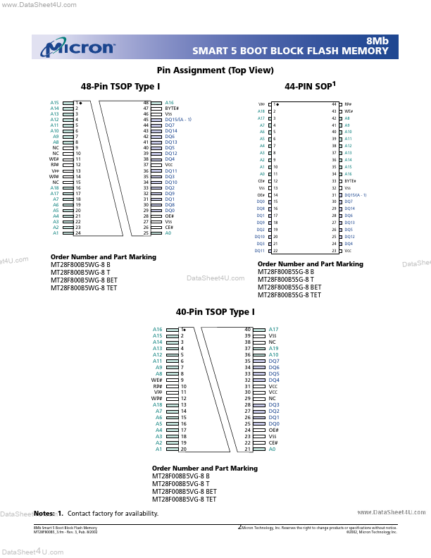
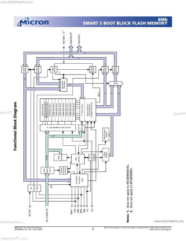
Due to process technology Boot Block Starting Word Address advances, 5V VPP is optimal for application and proTop T duction programming. These devices are fabricated Bottom B with Micron’s advanced 0.18µm CMOS floating-gate Operating Temperature Range process. mercial (0ºC to +70ºC) None The MT28F008B5 and MT28F800B5 are organized Extended (-40ºC to +85ºC) ET into eleven separately erasable blocks.
MT28F800B5 Key Features
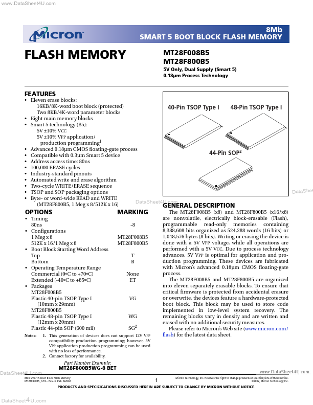
- Eleven erase blocks: 16KB/8K-word boot block (protected) 40-Pin TSOP Type I 48-Pin TSOP Type I Two 8KB/4K-word parameter
- Eight main memory blocks
- Advanced 0.18µm CMOS floating-gate process 44-Pin SOP2
- patible with 0.3µm Smart 5 device
- Address access time: 80ns
- 100,000 ERASE cycles
- Industry-standard pinouts
- Automated write and erase algorithm
- Two-cycle WRITE/ERASE sequence DataShee
- TSOP and SOP packaging options