Datasheet4U.com
🌙
M5M4V16169DTP-7 Datasheet | Mitsubishi Electric
Part:
M5M4V16169DTP-7
Description:
16M (1M-WORD BY 16-BIT) CACHED DRAM
Manufacturer:
Mitsubishi Electric
Size:
737.49 KB
M5M4V16169DTP-7 Datasheet (PDF) Download
Related M5M4V16169DTP-7 Datasheets
M5M4V16169DTP-8 16M (1M-WORD BY 16-BIT) CACHED DRAM
M5M4V16169DTP-10 16M (1M-WORD BY 16-BIT) CACHED DRAM
M5M4V16169DTP-15 16M (1M-WORD BY 16-BIT) CACHED DRAM
M5M4V16169DTP 16M (1M-WORD BY 16-BIT) CACHED DRAM
M5M4V16169DRT-10 16MCDRAM:16M(1M-WORD BY 16-BIT) CACHED DRAM WITH 16K (1024-WORD BY 16-BIT) SRAM
Mitsubishi Electric
M5M4V16169DTP-7
Description
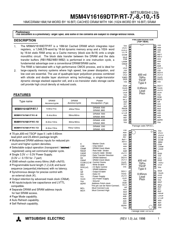
PINCONFIGURATION (TOP VIEW) 1.
×
Close