MC10141
MC10141 is Four Bit Universal Shift Register manufactured by Motorola Semiconductor.
MOTOROLA
SEMICONDUCTOR TECHNICAL DATA
Four Bit Universal Shift Register
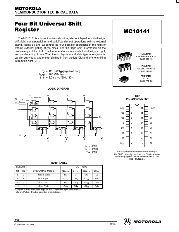
The MC10141 is a four- bit universal shift register which performs shift left, or shift right, serial/parallel in, and serial/parallel out operations with no external gating. Inputs S1 and S2 control the four possible operations of the register without external gating of the clock. The flip- flops shift information on the positive edge of the clock. The four operations are stop shift, shift left, shift right, and parallel entry of data. The other six inputs are all data type inputs; four for parallel entry data, and one for shifting in from the left (DL) and one for shifting in from the right (DR).
L SUFFIX CERAMIC PACKAGE CASE 620- 10 P SUFFIX PLASTIC PACKAGE CASE 648- 08 FN SUFFIX PLCC CASE 775- 02
PD = 425 m W typ/pkg (No Load) f Shift = 200 MHz typ tr, tf = 2.0 ns typ (20%- 80%)
LOGIC DIAGRAM
D3 S1 S2 1 of 4 Decoder Parallel Enter D2 D1 D0
DIP PIN ASSIGNMENT
VCC1 1 2 3 4 5 6 7 8 16 15 14 13 12 11 10 9 VCC2 Q1 Q0 DL D0 D1 S1 D2
Shift Right
Shift Left Hold DL
Q2 Q3 C
D Q C D Q C D Q C D Q C
DR D3 S2
C Q3 Q2 Q1 Q0
VCC1 = PIN 1 VCC2 = PIN 16 VEE = PIN 8
Pin assignment is for Dual- in- Line Package. For PLCC pin assignment, see the Pin Conversion Tables on page 6- 11 of the Motorola MECL Data Book (DL122/D).
TRUTH TABLE
SELECT S1 L L H H S2 L H L H OPERATING MODE Parallel Entry Shift Right- Shift Left- Stop Shift Q0n+1 D0 Q1n DL Q0n OUTPUTS Q1n+1 D1 Q2n Q0n Q1n Q2n+1 D2 Q3n Q1n Q2n Q3n+1 D3 DR Q2n Q3n
- Outputs as exist after pulse appears at “C” input with input conditions as shown. (Pulse = Positive transition of clock input).
3/93
© Motorola, Inc. 1996
3- 46
REV 5
SHIFT FREQUENCY TEST CIRCUIT
VCC1 = VCC2 +2.0 VDC
VOUT
COAX
25 u...