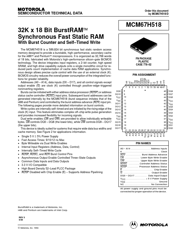
MCM67H518
feature eliminates plex off- chip write pulse generation and provides increased flexibility for ining signals. Dual write enables (LW and UW) are provided to allow individually writeable bytes. LW controls DQ0
- DQ8 (the lower bits), while UW controls DQ9
- DQ17 (the upper bits). This device is ideally suited for systems that require wide data bus widths and cache memory. See Figure 2 for applications information.
- -
- -
- -
- -
- -
- Single 5 V ± 5% Power Supply Fast Access Times: 9/10/12 ns Max Byte Writeable via Dual Write Enables Internal Input Registers (Address, Data, Control) Internally Self- Timed Write Cycle ADSP, ADSC, and ADV Burst Control Pins Asynchronous Output Enable Controlled Three- State Outputs mon Data Inputs and Data Outputs 3.3 V I/O patible High Board Density 52- Lead PLCC Package ADSP Disabled with Chip Enable (E)
- Supports Address Pipelining
FN PACKAGE PLASTIC CASE 778- 02
PIN ASSIGNMENT
A6 A7 E UW LW ADSC ADSP ADV K G A8 A9 A10 DQ9 DQ10 VCC VSS DQ11...