MMBFU310LT1 - JFET Transistor
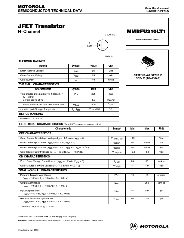
MOTOROLA SEMICONDUCTOR TECHNICAL DATA Order this document by MMBFU310LT1/D JFET Transistor N *Channel 2 SOURCE 3 GATE MMBFU310LT1 Motorola Preferred Device 1 DRAIN 3 1 2 MAXIMUM RATINGS Rating Drain *Source Voltage Gate *Source Voltage Gate Current Symbol VDS VGS IG Value 25 25 10 Unit Vdc Vdc mAdc CASE 318 * 08, STYLE 10 SOT * 23 (TO * 236AB) THERMAL CHARACTERISTICS Characteristic Total Device Dissipation FR * 5 Board(1) TA = 25°C Derat
MMBFU310LT1 Features
* g from preheating to soldering, the maximum temperature gradient shall be 5°C or less.
* After soldering has been completed, the device should be allowed to cool naturally for at least three minutes. Gradual cooling should be used as the use of forced cooling will increase the temperature gr