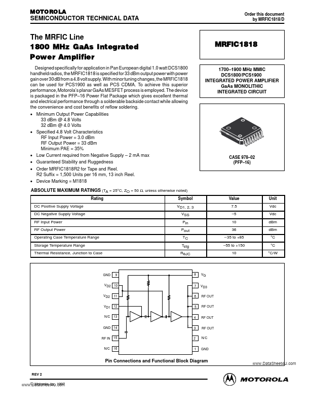
MRFIC1818
MRFIC1818 is 1800MHz GaAs Integrated Power Amplifier manufactured by Motorola Semiconductor.
( Data Sheet : .. )
MOTOROLA
SEMICONDUCTOR TECHNICAL DATA
Order this document by MRFIC1818/D
The MRFIC Line
1800 MHz Ga As Integrated Power Amplifier
Designed specifically for application in Pan European digital 1.0 watt DCS1800 handheld radios, the MRFIC1818 is specified for 33 d Bm output power with power gain over 30 d B from a 4.8 volt supply. With minor tuning changes, the MRFIC1818 can be used for PCS1900 as well as PCS CDMA. To achieve this superior performance, Motorola’s planar Ga As MESFET process is employed. The device is packaged in the PFP- 16 Power Flat Package which gives excellent thermal and electrical performance through a solderable backside contact while allowing the convenience and cost benefits of reflow soldering.
- Minimum Output Power Capabilities 33 d Bm @ 4.8 Volts 32 d Bm @ 4.0 Volts
- Specified 4.8 Volt Characteristics RF Input Power = 3.0 d Bm RF Output Power = 33 d Bm Minimum PAE = 35%
- Low Current required from Negative Supply
- 2 m A max
- Guaranteed Stability and Ruggedness
- Order MRFIC1818R2 for Tape and Reel. R2 Suffix = 1,500 Units per 16 mm, 13 inch Reel.
- Device Marking = M1818 ABSOLUTE MAXIMUM RATINGS (TA = 25°C, ZO = 50 Ω, unless otherwise noted)
Rating DC Positive Supply Voltage DC Negative Supply Voltage RF Input Power RF Output Power Operating Case Temperature Range Storage Temperature Range Thermal Resistance, Junction to Case Symbol VD1, 2, 3 VSS Pin Pout TC Tstg RθJC
1700- 1900 MHz MMIC DCS1800/PCS1900 INTEGRATED POWER AMPLIFIER Ga As MONOLITHIC INTEGRATED CIRCUIT
CASE 978- 02 (PFP- 16)
Value 7.5
- 5 10 36
- 35 to +85
- 55 to +150 10
Unit Vdc Vdc d Bm d Bm °C °C °C/W
8 7 6 5 4 3 2 1
VG VD3 RF OUT RF OUT RF OUT RF OUT N/C GND
VD2 10 VD2 11 VD1 12 N/C 13 GND 14 RF IN 15 N/C 16
Pin Connections and Functional Block Diagram
REV 2
..
MOTOROLA RF DEVICE DATA © Motorola, Inc. 1997 ..
MRFIC1818 1
REMENDED OPERATING RANGES
Parameter Supply Voltage Gate Voltage RF Frequency Range RF Input Power Symbol VD1, 2,...