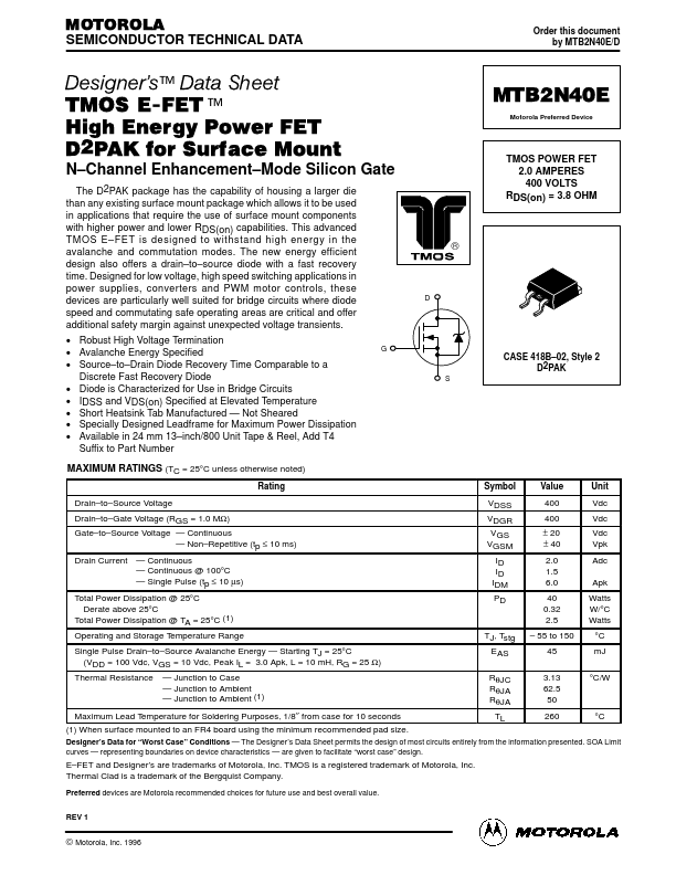
Datasheet4U Logo Datasheet4U.com

MTB2N40E - TMOS POWER FET

Features

  • f the curves would maintain a value of unity regardless of the switching speed. The circuit used to obtain the data is constructed to minimize common inductance in the drain and gate circuit loops and is believed readily achievable with board mounted components. Most power electronic loads are inductive; the data in the figure is taken with a resistive load, which approximates an optimally snubbed inductive load. Power MOSFETs may be safely operated into an inductive load; however, snubbing redu.

📥 Download Datasheet

Other Datasheets by Motorola

Full PDF Text Transcription

Click to expand full text
MOTOROLA SEMICONDUCTOR TECHNICAL DATA Order this document by MTB2N40E/D ™ Data Sheet TMOS E-FET.™ High Energy Power FET D2PAK for Surface Mount Designer's MTB2N40E Motorola Preferred Device N–Channel Enhancement–Mode Silicon Gate The D2PAK package has the capability of housing a larger die than any existing surface mount package which allows it to be used in applications that require the use of surface mount components with higher power and lower RDS(on) capabilities. This advanced TMOS E–FET is designed to withstand high energy in the avalanche and commutation modes. The new energy efficient design also offers a drain–to–source diode with a fast recovery time.
Published: |