Datasheet Summary
..
MOTOROLA
SEMICONDUCTOR TECHNICAL DATA
Order this document by MTP20N20E/D
Designer's
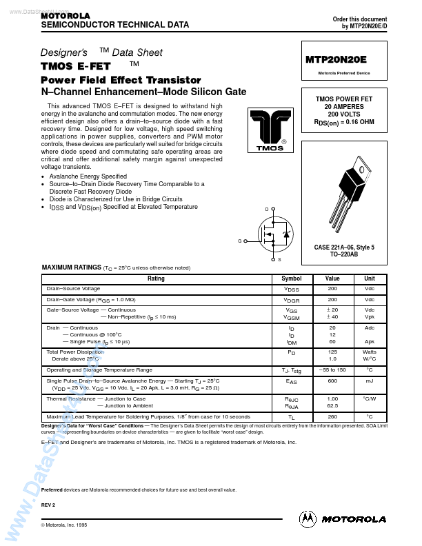
TMOS E-FET .™ Power Field Effect Transistor N- Channel Enhancement- Mode Silicon Gate
This advanced TMOS E- FET is designed to withstand high energy in the avalanche and mutation modes. The new energy efficient design also offers a drain- to- source diode with a fast recovery time. Designed for low voltage, high speed switching applications in power supplies, converters and PWM motor controls, these devices are particularly well suited for bridge circuits where diode speed and mutating safe operating areas are critical and offer additional safety margin against unexpected voltage...