2SK3305
2SK3305 is N-Channel MOSFET manufactured by NEC.
DESCRIPTION
The 2SK3305 is N-Channel DMOS FET device that features a low gate charge and excellent switching characteristics, and designed for high voltage applications such as switching power supply, AC adapter.
FEATURES
- Low gate charge: QG = 13 n C TYP. (VDD = 400 V, VGS = 10 V, ID = 5.0 A)
- Gate voltage rating: ±30 V
- Low on-state resistance RDS(on) = 1.5 Ω MAX. (VGS = 10 V, ID = 2.5 A)
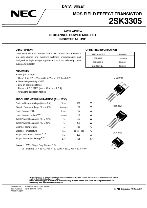
- Avalanche capability ratings (TO-220AB)
ABSOLUTE MAXIMUM RATINGS (TA = 25°C)
Drain to Source Voltage (VGS = 0 V) Gate to Source Voltage (VDS = 0 V) Drain Current (DC) Drain Current (pulse)
Note1
VDSS VGSS(AC) ID(DC) ID(pulse) PT PT Tch Tstg
500 ±30 ±5 ±20 75 1.5 150
- 55 to +150 5.0 125
V V A A W W °C °C A m J (TO-263) (TO-262)
Total Power Dissipation (TC = 25°C) Total Power Dissipation (TA = 25°C) Channel Temperature Storage Temperature Single Avalanche Current Single Avalanche Energy
Note2 Note2
IAS EAS
Notes 1. PW ≤ 10 µs, Duty Cycle ≤ 1 % 2. Starting Tch = 25 °C, VDD = 150 V, RG = 25 Ω, VGS = 20 V ¡ 0 V
The information in this document is subject to change without notice. Before using this document, please confirm that this is the latest version.
Not all devices/types available in every country. Please check with local NEC representative for availability and additional information.
Document No. D14003EJ1V0DS00 (1st edition) Date Published March 2000 NS CP(K) Printed in Japan
©
1998,2000
ELECTRICAL CHARACTERISTICS (TA = 25 °C)
CHARACTERISTICS Drain Leakage Current Gate to Source Leakage Current Gate to Source Cut-off Voltage Forward Transfer Admittance Drain to Source On-state Resistance Input Capacitance Output Capacitance Reverse Transfer Capacitance Turn-on Delay Time Rise Time Turn-off Delay Time Fall Time Total Gate Charge Gate to Source Charge Gate to Drain Charge Body Diode Forward Voltage Reverse Recovery Time Reverse Recovery Charge SYMBOL IDSS IGSS VGS(off) | yfs | RDS(on) Ciss Coss Crss td(on) tr td(off) tf QG QGS QGD VF(S-D) trr Qrr IF = 5.0...