UPA1800
UPA1800 is N-CHANNEL MOS FIELD EFFECT TRANSISTOR FOR SWITCHING manufactured by NEC.
DESCRIPTION
The µPA1800 is a switching device which can be driven directly by a 4.0-V power source. The µPA1800 features a low on-state resistance and excellent switching characteristics, and is suitable for applications such as power switch of portable machine and so on.
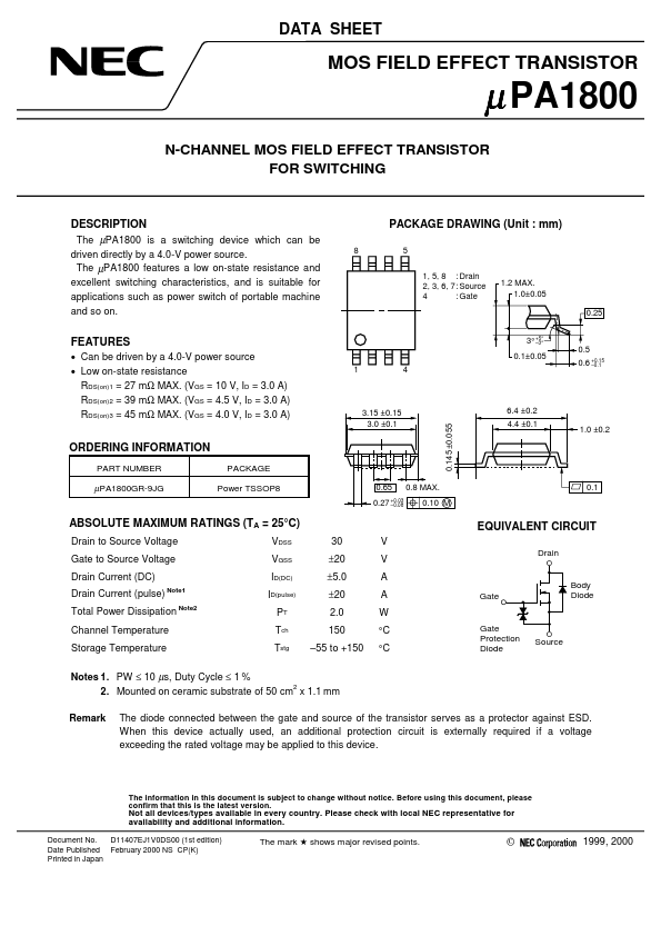
PACKAGE DRAWING (Unit : mm)
5 1, 5, 8 : Drain 2, 3, 6, 7: Source 4 : Gate
1.2 MAX. 1.0±0.05 0.25
° 3° +5
- 3°
FEATURES
- Can be driven by a 4.0-V power source
- Low on-state resistance RDS(on)1 = 27 mΩ MAX. (VGS = 10 V, ID = 3.0 A) RDS(on)2 = 39 mΩ MAX. (VGS = 4.5 V, ID = 3.0 A) RDS(on)3 = 45 mΩ MAX. (VGS = 4.0 V, ID = 3.0 A)
1 4
0.1±0.05
0.5 0.6 +0.15
- 0.1
0.145 ±0.055
3.15 ±0.15 3.0 ±0.1
6.4 ±0.2 4.4 ±0.1 1.0 ±0.2
ORDERING INFORMATION
PART NUMBER PACKAGE Power TSSOP8
0.65 0.27 +0.03
- 0.08 0.8 MAX.
µPA1800GR-9JG
0.10 M
ABSOLUTE MAXIMUM RATINGS (TA = 25°C)
Drain to Source Voltage Gate to Source Voltage Drain Current (DC) Drain Current (pulse)
Note1 Note2
EQUIVALENT CIRCUIT
30 ±20 ±5.0 ±20 2.0 150
- 55 to +150 V V A A W °C °C
Gate Protection Diode Source Gate Drain
VDSS VGSS ID(DC) ID(pulse) PT Tch Tstg
Body Diode
Total Power Dissipation Channel Temperature Storage Temperature
Notes 1. PW ≤ 10 µs, Duty Cycle ≤ 1 % 2 2. Mounted on ceramic substrate of 50 cm x 1.1 mm Remark The diode connected between the gate and source of the transistor serves as a protector against ESD. When this device actually used, an additional protection circuit is externally required if a voltage exceeding the rated voltage may be applied to this device.
The information in this document is subject to change without notice. Before using this document, please confirm that this is the latest version.
Not all devices/types available in every country. Please check with local NEC representative for availability and additional information.
Document No. D11407EJ1V0DS00 (1st edition) Date Published February 2000 NS CP(K) Printed in Japan
The mark 5 shows major revised...