Datasheet4U Logo Datasheet4U.com

UPD44164362 - (UPD44164082/182/362) 18M-BIT DDRII SRAM 2-WORD BURST OPERATION

This page provides the datasheet information for the UPD44164362, a member of the UPD44164082 (UPD44164082/182/362) 18M-BIT DDRII SRAM 2-WORD BURST OPERATION family.

Datasheet Summary

Description

technology using full CMOS six-transistor memory cell.

Features

  • 1.8 ± 0.1 V power supply and HSTL I/O.
  • DLL circuitry for wide output data valid window and future frequency scaling.
  • Pipelined double data rate operation.
  • Common data input/output bus.
  • Two-tick burst for low DDR transaction size.
  • Two input clocks (K and /K) for precise DDR timing at clock rising edges only.
  • Two output clocks (C and /C) for precise flight time and clock skew matching-clock and data delivered together to receiving dev.

📥 Download Datasheet

Datasheet preview – UPD44164362

Datasheet Details

Part number UPD44164362
Manufacturer NEC
File Size 282.71 KB
Description (UPD44164082/182/362) 18M-BIT DDRII SRAM 2-WORD BURST OPERATION
Datasheet download datasheet UPD44164362 Datasheet
Additional preview pages of the UPD44164362 datasheet.
Other Datasheets by NEC

Full PDF Text Transcription

Click to expand full text
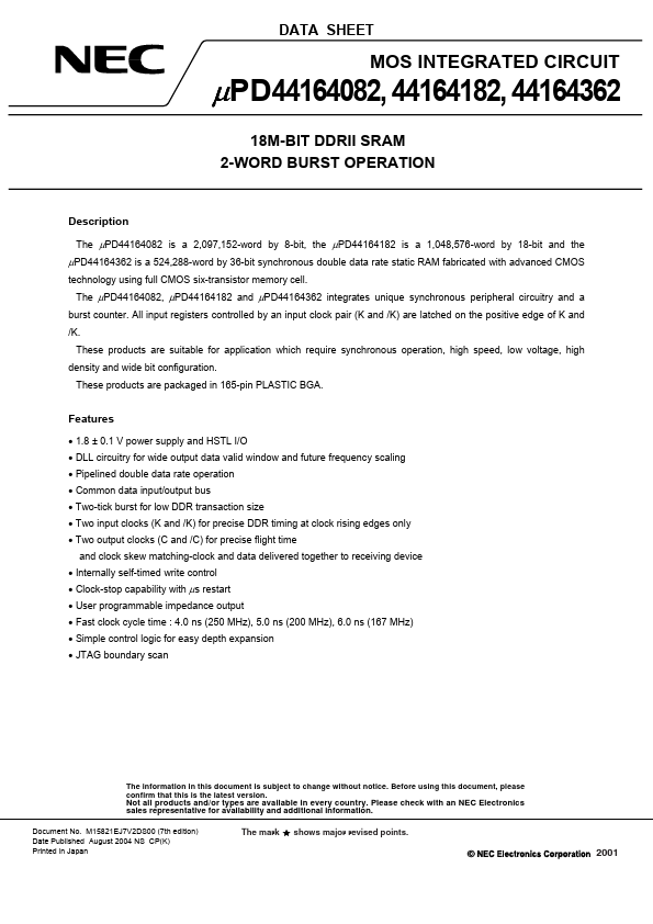
DATA SHEET MOS INTEGRATED CIRCUIT µPD44164082, 44164182, 44164362 18M-BIT DDRII SRAM 2-WORD BURST OPERATION Description The µPD44164082 is a 2,097,152-word by 8-bit, the µPD44164182 is a 1,048,576-word by 18-bit and the µPD44164362 is a 524,288-word by 36-bit synchronous double data rate static RAM fabricated with advanced CMOS technology using full CMOS six-transistor memory cell. The µPD44164082, µPD44164182 and µPD44164362 integrates unique synchronous peripheral circuitry and a burst counter. All input registers controlled by an input clock pair (K and /K) are latched on the positive edge of K and /K. These products are suitable for application which require synchronous operation, high speed, low voltage, high density and wide bit configuration.
Published: |