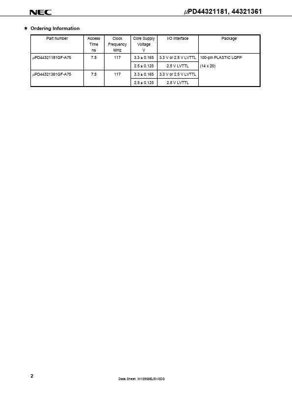
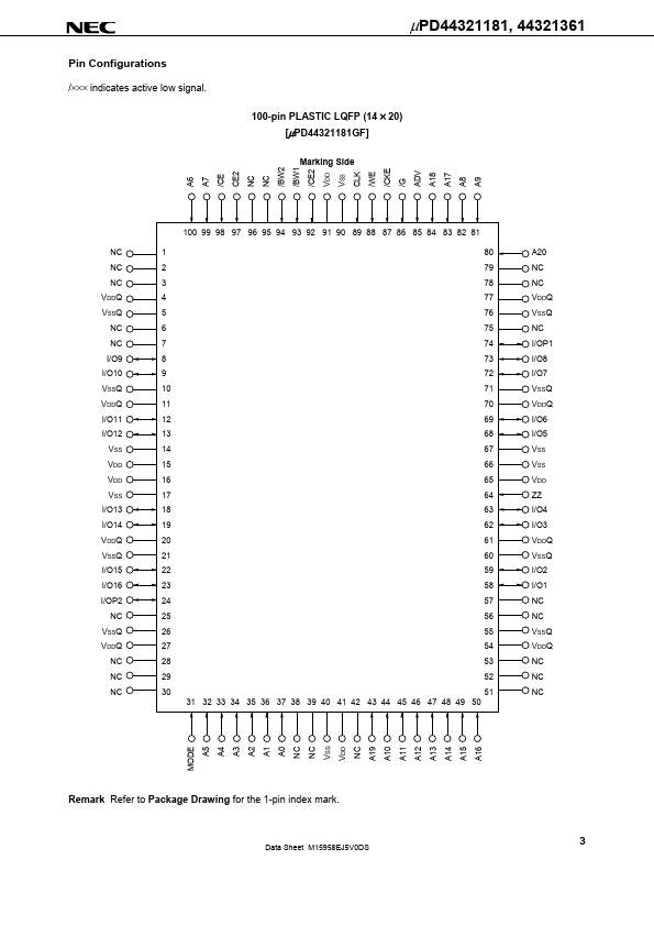
Datasheet4U Logo Datasheet4U.com

UPD44321361 - (UPD44321181 / UPD44321361) 32M-BIT ZEROSB SRAM FLOW THROUGH OPERATION

Download the UPD44321361 datasheet PDF. This datasheet also covers the UPD44321181 variant, as both devices belong to the same (upd44321181 / upd44321361) 32m-bit zerosb sram flow through operation family and are provided as variant models within a single manufacturer datasheet.

Description

The µPD44321181 is a 2,097,152-word by 18-bit and the µPD44321361 is a 1,048,576-word by 36-bit ZEROSB static RAM fabricated with advanced CMOS technology using full CMOS six-transistor memory cell.

Features

  • Low voltage core supply: VDD = 3.3 ± 0.165 V / 2.5 ± 0.125 V.
  • Synchronous operation.
  • 100 percent bus utilization.
  • Internally self-timed write control.
  • Burst read / write : Interleaved burst and linear burst sequence.
  • Fully registered inputs and outputs for flow through operation.
  • All registers triggered off positive clock edge.
  • 3.3V or 2.5V LVTTL Compatible : All inputs and outputs.
  • Fast clock access time : 7.5 ns.

📥 Download Datasheet

Note: The manufacturer provides a single datasheet file (UPD44321181_NEC.pdf) that lists specifications for multiple related part numbers.

Datasheet Details

Part number UPD44321361
Manufacturer NEC
File Size 318.26 KB
Description (UPD44321181 / UPD44321361) 32M-BIT ZEROSB SRAM FLOW THROUGH OPERATION
Datasheet download datasheet UPD44321361 Datasheet

Full PDF Text Transcription

Click to expand full text
www.DataSheet4U.com DATA SHEET MOS INTEGRATED CIRCUIT µ PD44321181, 44321361 32M-BIT ZEROSBTM SRAM FLOW THROUGH OPERATION Description The µPD44321181 is a 2,097,152-word by 18-bit and the µPD44321361 is a 1,048,576-word by 36-bit ZEROSB static RAM fabricated with advanced CMOS technology using full CMOS six-transistor memory cell. The µPD44321181 and µPD44321361 are optimized to eliminate dead cycles for read to write, or write to read transitions. These ZEROSB static RAMs integrate unique synchronous peripheral circuitry, 2-bit burst counter and output buffer as well as SRAM core. All input registers are controlled by a positive edge of the single clock input (CLK).
Published: |