74AHC132
Description
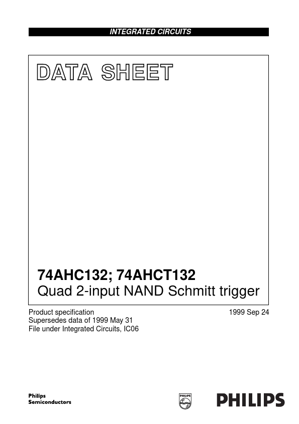
data inputs data inputs data outputs ground (0 V) DC supply voltage handbook, halfpage 1 1A 1Y 3 2 handbook, halfpage 1B 1A 1B 1Y 2A 2B 2Y GND 1 2 3 4 5 6 7 MNA406 14 VCC 13 4B 12 4A 5 4 2A 2Y 2B 6 132 11 4Y 10 3B 9 3A 10 3B 9 3A 3Y 8 8 3Y 12 4A 4Y 11 13 4B MNA407 Fig.1 Pin configuration. Fig.2 Logic symbol. 1999 Sep 24 3 Philips Semiconductors Product specification Quad 2-input NAND Schmitt trigger 74AHC132; 74AHCT132 handbook, halfpage 1 2 4 5 9 10 12 13 & 3 & 6 handbook, halfpage A Y & 8 B MNA409 & 11 MNA408 Fig.3 IEC logic symbol.
Key Features
- ESD protection: HBM EIA/JESD22-A114-A exceeds 2000 V; MM EIA/JESD22-A115-A exceeds 200 V CDM EIA/JESD22-C101 exceeds 1000 V
- Balanced propagation delays
- Inputs accepts voltages higher than VCC
- For AHC only: operates with CMOS input levels
- For AHCT only: operates with TTL input levels
- Specified from -40 to +85 and +125 °C. DESCRIPTION The 74AHC/AHCT132 are high-speed Si-gate CMOS devices and are pin compatible with Low power Schottky TTL (LSTTL). They are specified in compliance with JEDEC standard No. 7A. The 74AHC/AHCT132 contain four 2-input NAND gates which accept standard input signals. They are capable of transforming slowly changing input signals into sharply defined, jitter free output signals. The gate switches at different points for positive and negative-going signals. The difference between the positive voltage VT+ and the negative VT- is defined as the hysteresis voltage VH. ORDERING INFORMATION OUTSIDE NORTH AMERICA 74AHC132D 74AHC132PW 74AHCT132D 74AHCT132PW Note FUNCTION TABLE See note 1. INPUTS nA L L H H 74AHC132; 74AHCT132 OUTPUT nB L H L H nY H H H L 1. H = HIGH voltage level; L = LOW voltage level. QUICK REFERENCE DATA GND = 0 V; Tamb = 25 °C; tr = tf ≤ 3.0 ns. TYPICAL SYMBOL tPHL/tPLH CI CO CPD PARAMETER propagation delay nA to nY input capacitance output capacitance power dissipation capacitance CL = 50 pF; f = 1 MHz; notes 1 and 2 CONDITIONS AHC CL = 15 pF; VCC = 5 V VI = VCC or GND 3.3 3.0 4.0 11 AHCT 3.5 3.0 4.0 14 ns pF pF pF UNIT Notes 1. CPD is used to determine the dynamic power dissipation (PD in µW). PD = CPD × VCC2 × fi + ∑ (CL × VCC2 × fo) where: fi = input frequency in MHz; fo = output frequency in MHz; ∑ (CL × VCC2 × fo) = sum of outputs; CL = output load capacitance in pF; VCC = supply voltage in Volts. 2. The condition is VI = GND to VCC.