MW7IC2750NR1
Features
- 100% PAR Tested for Guaranteed Output Power Capability
- Characterized with Series Equivalent Large--Signal Impedance Parameters and mon Source S--Parameters
- On--Chip Matching (50 Ohm Input, DC Blocked)
- Integrated Quiescent Current Temperature pensation with Enable/Disable Function (1)
- Integrated ESD Protection
- Greater Negative Gate--Source Voltage Range for Improved Class C Operation
- 225°C Capable Plastic Package
- In Tape and Reel. R1 Suffix = 500 Units, 44 mm Tape Width, 13 inch Reel.
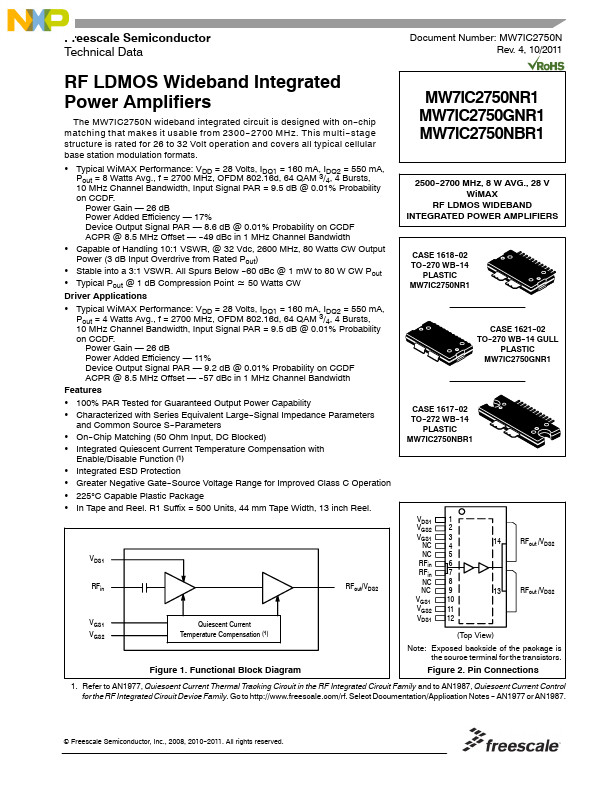
VDS1 RFin
RFout/VDS2
VGS1
Quiescent Current
VGS2
Temperature pensation (1)
Figure 1. Functional Block Diagram
MW7IC2750NR1 MW7IC2750GNR1 MW7IC2750NBR1
2500--2700 MHz, 8 W AVG., 28 V Wi MAX
RF LDMOS WIDEBAND INTEGRATED POWER AMPLIFIERS
CASE 1618--02 TO--270 WB--14
PLASTIC MW7IC2750NR1
CASE 1621--02 TO--270 WB--14 GULL
PLASTIC MW7IC2750GNR1
CASE 1617--02 TO--272 WB--14
PLASTIC MW7IC2750NBR1
VDS1
VGS2
VGS1
NC 4
NC 5
RFin 6 RFin 7
NC 8
NC 9
VGS1 10
VGS2...