N32T1630C1C
Overview
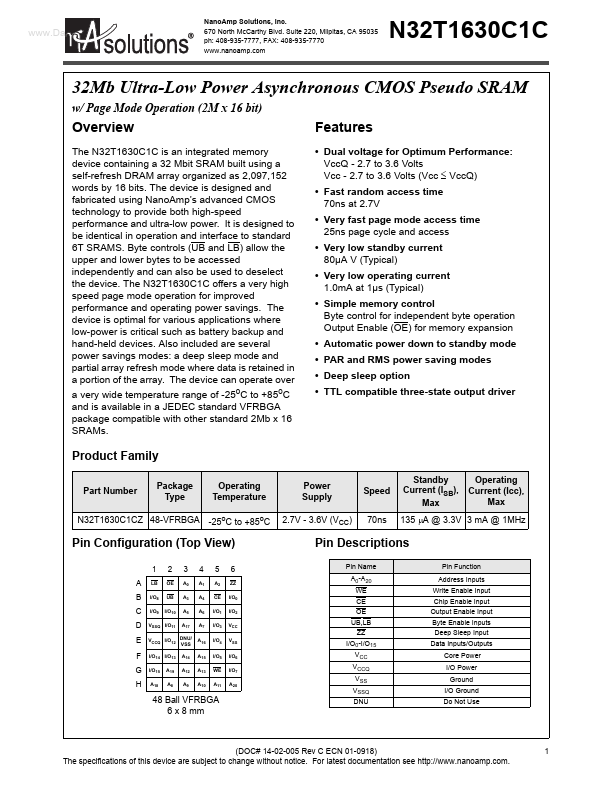
The N32T1630C1C is an integrated memory device containing a 32 Mbit SRAM built using a self-refresh DRAM array organized as 2,097,152 words by 16 bits. The device is designed and fabricated using Nano Amp’s advanced CMOS technology to provide both high-speed performance and ultra-low power. It is designed to be identical in operation and interface to standard 6T SRAMS. Byte controls (UB and LB) allow the upper and lower bytes to be accessed independently and can also be used to deselect the device. The N32T1630C1C offers a very high speed page mode operation for improved performance and operating power savings. The device is optimal for various applications where low-power is critical such as battery backup and hand-held devices. Also included are several power savings modes: a deep sleep mode and partial array refresh mode where data is retained in a portion of the array. The device can operate over a very wide temperature range of -25o C to +85o C and is available in a JEDEC...