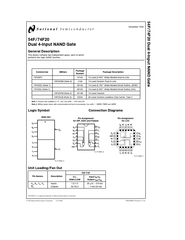
Datasheet4U Logo Datasheet4U.com

74F20 Datasheet Dual 4-Input NAND Gate

Manufacturer: National

Overview: 54F 74F20 Dual 4-Input NAND Gate November 1994 54F 74F20 Dual 4-Input NAND.

Datasheet Details

Part number 74F20
Manufacturer National
File Size 140.04 KB
Description Dual 4-Input NAND Gate
Download 74F20 Download (PDF)

General Description

This device contains two independent gates each of which performs the logic NAND function Commercial 74F20PC Military Package Number N14A Package Description 14-Lead (0 300 Wide) Molded Dual-In-Line 14-Lead Ceramic Dual-In-Line 14-Lead (0 150 Wide) Molded Small Outline JEDEC 14-Lead (0 300 Wide) Molded Small Outline EIAJ 14-Lead Cerpack 20-Lead Ceramic Leadless Chip Carrier Type C 54F20DM (Note 2) 74F20SC (Note 1) 74F20SJ (Note 1) 54F20FM (Note 2) 54F20LM (Note 2) J14A M14A M14D W14B E20A Note 1 Devices also available in 13 reel Use suffix e SCX and SJX Note 2 Military grade device with environmental and burn-in processing Use suffix e DMQB FMQB and LMQB Logic Symbol IEEE IEC Connection Diagrams Pin Assignment for DIP SOIC and Flatpak Pin Assignment for LCC TL F 9462 – 2 TL F 9462 – 1 TL F 9462–3 Unit Loading Fan Out 54F 74F Pin Names Description UL HIGH LOW 10 10 50 33 3 Input IIH IIL Output IOH IOL 20 mA b0 6 mA b 1 mA 20 mA An Bn Cn Dn On Inputs Outputs TRI-STATE is a registered trademark of National Semiconductor Corporation C1995 National Semiconductor Corporation TL F 9462 RRD-B30M75 Printed in U S A Absolute Maximum Ratings (Note 1) If Military Aerospace specified devices are required please contact the National Semiconductor Sales Office Distributors for availability and specifications Storage Temperature Ambient Temperature under Bias Junction Temperature under Bias Plastic VCC Pin Potential to Ground Pin b 65 C to a 150 b 55 C to a 125 b 55 C to a 175 b 55 C to a 150 Recommended Operating Conditions Free Air Ambient Temperature Military Commercial Supply Voltage Military Commercial b 55 C to a 125 C 0 C to a 70 C a 4 5V to a 5 5V a 4 5V to a 5 5V C C C C b 0 5V to a 7 0V b 0 5V to a 7 0V Input Voltage (Note 2) b 30 mA to a 5 0 mA Input Current (Note 2) Voltage Applied to Output in HIGH State (with VCC e 0V) b 0 5V to VCC Standard Output