74ACT169
74ACT169 is 4-Stage Synchronous Bidirectional Counter manufactured by National Semiconductor.
- Part of the 74AC169 comparator family.
- Part of the 74AC169 comparator family.
Description
The ’AC ’ACT169 is fully synchronous 4-stage up down counter The ’AC ’ACT169 is a modulo-16 binary counter It features a preset capability for programmable operation carry lookahead for easy cascading and a U D input to control the direction of counting All state changes whether in counting or parallel loading are initiated by the LOW-to HIGH transition of the Clock
Features
Y ICC reduced by 50% Y Synchronous counting and loading Y Built-In lookahead carry capability Y Presettable for programmable operation Y Outputs source sink 24 m A Y ’ACT has TTL-patible inputs Y Standard Military Drawing (SMD)
’AC169 5962-91603
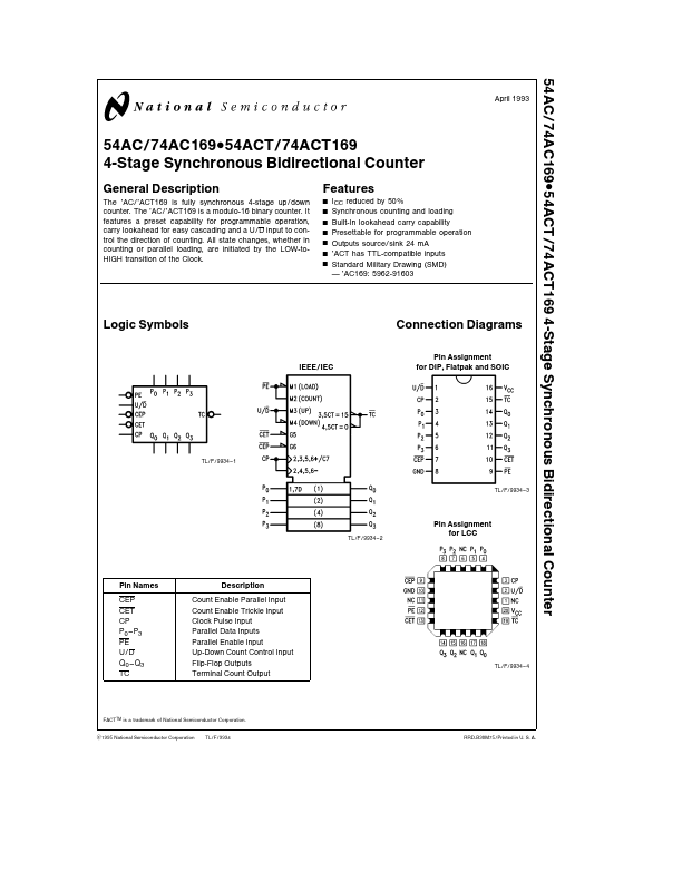
Logic Symbols
IEEE IEC
Connection Diagrams
Pin Assignment for DIP Flatpak and SOIC
TL F 9934- 1
Pin Names
CEP CET CP P0
- P3 PE UD Q0
- Q3 TC
Description
Count Enable Parallel Input Count Enable Trickle Input Clock Pulse Input Parallel Data Inputs Parallel Enable Input Up-Down Count Control Input Flip-Flop Outputs Terminal Count Output
FACTTM is a trademark of National Semiconductor Corporation C1995 National Semiconductor Corporation TL F 9934
TL F 9934
- 2
TL F 9934
- 3
Pin Assignment for LCC
TL F 9934
- 4 RRD-B30M75 Printed in U S A
Logic Diagram
TL F 9934
- 5 Please note that this diagram is provided only for the understanding of logic operations and should not be used to estimate propagation delays
Functional Description
The ’AC ’ACT169 uses edge-triggered J-K-type flip-flops and have no constraints on changing the control or data input signals in either state of the Clock The only requirement is that the various inputs attain the desired state at least a setup time before the rising edge of the clock and remain valid for the remended hold time thereafter The parallel load operation takes precedence over the other operations as indicated in the Mode Select Table When PE is LOW the data on the P0
- P3 inputs enters the flip-flops on the next rising edge of the Clock In order for counting to occur both CEP and CET must be LOW...