74C173
74C173 is TRI-STATE Quad D Flip-Flop manufactured by National Semiconductor.
MM54C173 MM74C173 TRI-STATE Quad D Flip-Flop
February 1988
MM54C173 MM74C173 TRI-STATE Quad D Flip-Flop
General Description
The MM54C173 MM74C173 TRI-STATE quad D flip-flop is a monolithic plementary MOS (CMOS) integrated circuit constructed with N- and P-channel enhancement transistors The four D-type flip-flops operate synchronously from a mon clock The TRI-STATE output allows the device to be used in bus-organized systems The outputs are placed in the TRI-STATE mode when either of the two output disable pins are in the logic ‘‘1’’ level The input disable allows the flip-flops to remain in their present states without disrupting the clock If either of the two input disables are taken to a logic ‘‘1’’ level the Q outputs are fed back to the inputs and in this manner the flip-flops do not change state Clearing is enabled by taking the input to a logic ‘’1’’ level Clocking occurs on the positive-going transition
Features
Y Y Y Y Y Y Y
Supply voltage range 3V to 15V Tenth power TTL patible Drive 2 LPTTL loads High noise immunity 0 45 VCC (typ ) Low power Medium speed operation High impedance TRI-STATE Input disable without gating the clock
Applications
Automotive Data terminals Instrumentation Medical electronics
Alarm systems Industrial electronics Remote metering puters
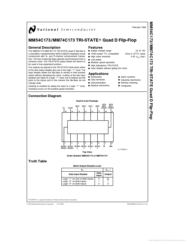
Connection Diagram
Dual-In-Line Package
TL F 5898
- 2
Top View Order Number MM54C173 or MM74C173
Truth Table
(Both Output Disables Low) tn Data Input Disable Logic ‘‘1’’ on One or Both Inputs Logic ‘‘0’’ on Both Inputs Logic ‘‘0’’ on Both Inputs Data Input X 1 0 tn a 1 Output Qn 1 0
TRI-STATE is a registered trademark of National Semiconductor Corporation C1995 National Semiconductor Corporation TL F 5898 RRD-B30M105 Printed in U S A
Free Datasheet...