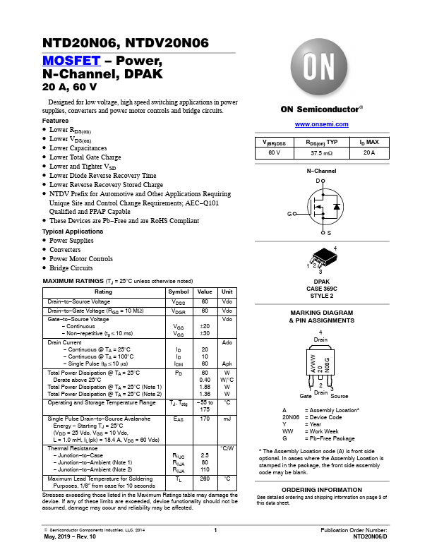
NTD20N06, NTDV20N06
MOSFET – Power,
N-Channel, DPAK
20 A, 60 V
Designed for low voltage, high speed switching applications in power
supplies, converters and power motor controls and bridge circuits.
Features
• Lower RDS(on)
• Lower VDS(on)
• Lower Capacitances
• Lower Total Gate Charge
• Lower and Tighter VSD
• Lower Diode Reverse Recovery Time
• Lower Reverse Recovery Stored Charge
• NTDV Prefix for Automotive and Other Applications Requiring
Unique Site and Control Change Requirements; AEC−Q101
Qualified and PPAP Capable
• These Devices are Pb−Free and are RoHS Compliant
Typical Applications
• Power Supplies
• Converters
• Power Motor Controls
• Bridge Circuits
MAXIMUM RATINGS (TJ = 25°C unless otherwise noted)
Rating
Symbol Value Unit
Drain−to−Source Voltage
Drain−to−Gate Voltage (RGS = 10 MW)
Gate−to−Source Voltage
− Continuous
− Non−repetitive (tpv10 ms)
Drain Current
− Continuous @ TA = 25°C
− Continuous @ TA = 100°C
− Single Pulse (tpv10 ms)
Total Power Dissipation @ TA = 25°C
Derate above 25°C
Total Power Dissipation @ TA = 25°C (Note 1)
Total Power Dissipation @ TA = 25°C (Note 2)
Operating and Storage Temperature Range
VDSS
VDGR
VGS
VGS
ID
ID
IDM
PD
TJ, Tstg
60
60
±20
±30
20
10
60
60
0.40
1.88
1.36
−55 to
175
Vdc
Vdc
Vdc
Adc
Apk
W
W/°C
W
W
°C
Single Pulse Drain−to−Source Avalanche
Energy − Starting TJ = 25°C
(VDD = 25 Vdc, VGS = 10 Vdc,
L = 1.0 mH, IL(pk) = 18.4 A, VDS = 60 Vdc)
Thermal Resistance
− Junction−to−Case
− Junction−to−Ambient (Note 1)
− Junction−to−Ambient (Note 2)
Maximum Lead Temperature for Soldering
Purposes, 1/8″ from case for 10 seconds
EAS
RqJC
RqJA
RqJA
TL
170 mJ
°C/W
2.5
80
110
260 °C
Stresses exceeding those listed in the Maximum Ratings table may damage the
device. If any of these limits are exceeded, device functionality should not be
assumed, damage may occur and reliability may be affected.
www.onsemi.com
V(BR)DSS
60 V
RDS(on) TYP
37.5 mW
ID MAX
20 A
N−Channel
D
G
S
4
12
3
DPAK
CASE 369C
STYLE 2
MARKING DIAGRAM
& PIN ASSIGNMENTS
4
Drain
1
Gate
2
Drain
3
Source
A
20N06
Y
WW
G
= Assembly Location*
= Device Code
= Year
= Work Week
= Pb−Free Package
* The Assembly Location code (A) is front side
optional. In cases where the Assembly Location is
stamped in the package, the front side assembly
code may be blank.
ORDERING INFORMATION
See detailed ordering and shipping information on page 3 of
this data sheet.
© Semiconductor Components Industries, LLC, 2014
1
May, 2019 − Rev. 10
Publication Order Number:
NTD20N06/D