2N3906
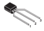
Representative 2N3906 image (package may vary by manufacturer)
Overview
- Pb-Free Packages are Available*
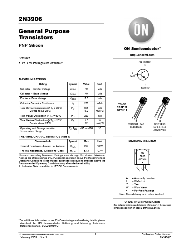
| Part | 2N3906 |
|---|---|
| Description | PNP General-Purpose Amplifier |
| Manufacturer | onsemi |
| Size | 247.42 KB |
Representative 2N3906 image (package may vary by manufacturer)
| Part Number | Manufacturer | Description |
|---|---|---|
| 2N3906 | NXP Semiconductors | PNP switching transistor |
| 2N3906 | STMicroelectronics | SMALL SIGNAL PNP TRANSISTOR |
| 2N3906 | Kodenshi AUK Group | PNP Silicon Transistor |
| 2N3906S | KEC | EPITAXIAL PLANAR PNP TRANSISTOR |
| 2N3906S | Inchange Semiconductor | PNP Transistor |