2N5551TA
Overview
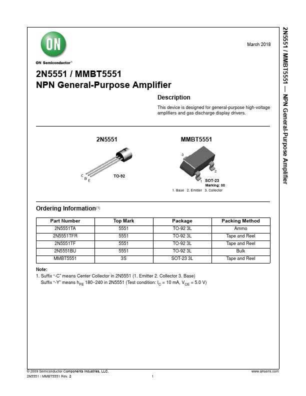
This device is designed for general-purpose high-voltage amplifiers and gas discharge display drivers. 2N5551 MMBT5551 3 TO-92 2 1 SOT-23.
| Part | 2N5551TA |
|---|---|
| Description | NPN Amplifier |
| Manufacturer | onsemi |
| Size | 283.56 KB |
This device is designed for general-purpose high-voltage amplifiers and gas discharge display drivers. 2N5551 MMBT5551 3 TO-92 2 1 SOT-23.
| Part Number | Manufacturer | Description |
|---|---|---|
| 2N5551 | Fairchild Semiconductor | NPN General Purpose Amplifier |
| 2N5551 | Philips Semiconductors | NPN high-voltage transistors |
| 2N5551 | Multicomp | Bipolar Transistor |
| 2N5551 | SeCoS Halbleitertechnologie GmbH | NPN Transistor |
| 2N5551 | Motorola Semiconductor | Amplifier Transistors |