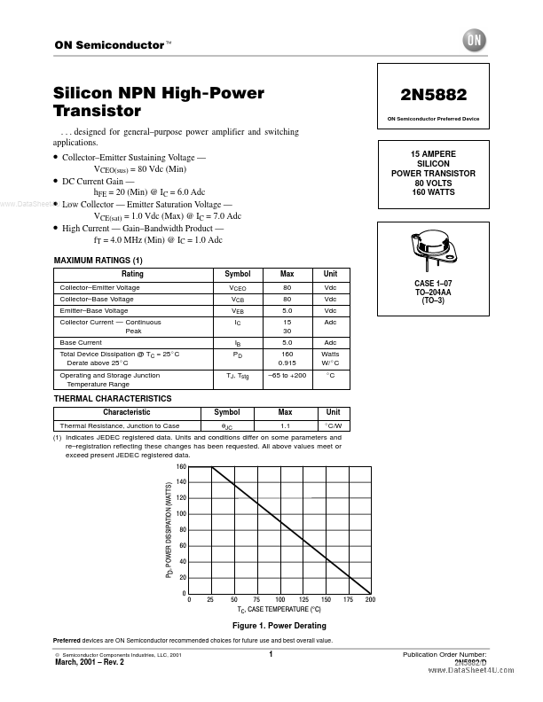
2N5882
ÎÎÎÎÎÎÎÎÎÎÎÎÎÎÎÎÎÎÎÎÎÎÎÎÎÎÎÎÎÎÎÎÎ*ELECTRICAL CHARACTERISTICS (TC = 25_C unless otherwise noted)
ÎÎÎÎÎÎÎÎÎÎÎÎÎÎÎÎÎÎÎÎÎÎÎÎÎÎÎÎÎÎÎÎÎCharacteristic
ÎÎÎÎÎÎÎÎÎÎÎÎÎÎÎÎÎÎÎÎÎÎÎÎÎÎÎÎÎÎÎÎÎOFF CHARACTERISTICS
Collector–Emitter Sustaining Voltage (2)
ÎÎÎÎÎÎÎÎÎÎÎÎÎÎÎÎÎÎÎÎÎÎÎÎÎÎÎÎÎÎÎÎÎ(IC = 200 mAdc, IB = 0)
ÎÎÎÎÎÎÎÎÎÎÎÎÎÎÎÎÎÎÎÎÎÎÎÎÎÎÎÎÎÎÎÎÎCollector Cutoff Current
ÎÎÎÎÎÎÎÎÎÎÎÎÎÎÎÎÎÎÎÎÎÎÎÎÎÎÎÎÎÎÎÎÎ(VCE = 40 Vdc, IB = 0)
ÎÎÎÎÎÎÎÎÎÎÎÎÎÎÎÎÎÎÎÎÎÎÎÎÎÎÎÎÎÎÎÎÎCollector Cutoff Current
(VCE = 80 Vdc, VBE(off) = 1.5 Vdc)
ÎÎÎÎÎÎÎÎÎÎÎÎÎÎÎÎÎÎÎÎÎÎÎÎÎÎÎÎÎÎÎÎÎ(VCE = 80 Vdc, VBE(off) = 1.5 Vdc, TC = 150_C)
ÎÎÎÎÎÎÎÎÎÎÎÎÎÎÎÎÎÎÎÎÎÎÎÎÎÎÎÎÎÎÎÎÎCollector Cutoff Current
ÎÎÎÎÎÎÎÎÎÎÎÎÎÎÎÎÎÎÎÎÎÎÎÎÎÎÎÎÎÎÎÎÎ(VCB = 80 Vdc, IE = 0)
ÎÎÎÎÎÎÎÎÎÎÎÎÎÎÎÎÎÎÎÎÎÎÎÎÎÎÎÎÎÎÎÎÎEmitter Cutoff Current (VEB = 5.0 Vdc, IC = 0)
ON CHARACTERISTICS
ÎÎÎÎÎÎÎÎÎÎÎÎÎÎÎÎÎÎÎÎÎÎÎÎÎÎÎÎÎÎÎÎÎwww.DataSheet4UD.cComCurrent Gain (1)
ÎÎÎÎÎÎÎÎÎÎÎÎÎÎÎÎÎÎÎÎÎÎÎÎÎÎÎÎÎÎÎÎÎ(IC = 2.0 Adc, VCE = 4.0 Vdc)
ÎÎÎÎÎÎÎÎÎÎÎÎÎÎÎÎÎÎÎÎÎÎÎÎÎÎÎÎÎÎÎÎÎ(IC = 6.0 Adc, VCE = 4.0 Vdc)
(IC = 15 Adc, VCE = 4.0 Vdc)
ÎÎÎÎÎÎÎÎÎÎÎÎÎÎÎÎÎÎÎÎÎÎÎÎÎÎÎÎÎÎÎÎÎCollector–Emitter Saturation Voltage (2)
ÎÎÎÎÎÎÎÎÎÎÎÎÎÎÎÎÎÎÎÎÎÎÎÎÎÎÎÎÎÎÎÎÎ(IC =7.0Adc,IB =0.7Adc)
(IC = 15 Adc, IB = 3.75 Adc)
ÎÎÎÎÎÎÎÎÎÎÎÎÎÎÎÎÎÎÎÎÎÎÎÎÎÎÎÎÎÎÎÎÎBase–Emitter Saturation Voltage (1) (IC = 15 Adc, IB = 3.75 Adc)
ÎÎÎÎÎÎÎÎÎÎÎÎÎÎÎÎÎÎÎÎÎÎÎÎÎÎÎÎÎÎÎÎÎBase–Emitter On Voltage (2) (IC = 6.0 Adc, VCE = 4.0 Vdc)
ÎÎÎÎÎÎÎÎÎÎÎÎÎÎÎÎÎÎÎÎÎÎÎÎÎÎÎÎÎÎÎÎÎDYNAMIC CHARACTERISTICS
ÎÎÎÎÎÎÎÎÎÎÎÎÎÎÎÎÎÎÎÎÎÎÎÎÎÎÎÎÎÎÎÎÎCurrent–Gain — Bandwidth Product (3)
ÎÎÎÎÎÎÎÎÎÎÎÎÎÎÎÎÎÎÎÎÎÎÎÎÎÎÎÎÎÎÎÎÎ(IC = 1.0 Adc, VCE = 10 Vdc, ftest = 1.0 MHz)
Output Capacitance
ÎÎÎÎÎÎÎÎÎÎÎÎÎÎÎÎÎÎÎÎÎÎÎÎÎÎÎÎÎÎÎÎÎ(VCB = 10 Vdc, IE = 0, f = 100 kHz)
ÎÎÎÎÎÎÎÎÎÎÎÎÎÎÎÎÎÎÎÎÎÎÎÎÎÎÎÎÎÎÎÎÎSmall–Signal Current Gain (IC = 2.0 Adc, VCE = 4.0 Vdc, f = 1.0 kHz)
ÎÎÎÎÎÎÎÎÎÎÎÎÎÎÎÎÎÎÎÎÎÎÎÎÎÎÎÎÎÎÎÎÎSWITCHING CHARACTERISTICS
ÎÎÎÎÎÎÎÎÎÎÎÎÎÎÎÎÎÎÎÎÎÎÎÎÎÎÎÎÎÎÎÎÎRise Time
Storage Time
ÎÎÎÎÎÎÎÎÎÎÎÎÎÎÎÎÎÎÎÎÎÎÎÎÎÎÎÎÎÎÎÎÎÎÎÎÎÎÎÎÎÎÎÎÎÎÎÎÎÎÎÎÎÎÎÎÎÎÎÎÎÎÎÎÎÎFall Time
(VCC = 30 Vdc, IC = 6.0 Adc,
IB1 = IB2 = 0.6 Adc See Figure 2)
Symbol
VCEO(sus)
ICEO
ICEX
ICBO
IEBO
hFE
VCE(sat)
VBE(sat)
VBE(on)
fT
Cob
hfe
tr
ts
tf
Min
80
—
—
—
—
—
35
20
4.0
—
—
—
—
4.0
—
20
—
—
—
Max Unit
Vdc
—
mAdc
1.0
mAdc
0.5
5.0
mAdc
0.5
1.0 mAdc
—
—
100
—
Vdc
1.0
4.0
2.5 Vdc
1.5 Vdc
— MHz
pF
400
——
0.7 µs
1.0 µs
0.8 µs
*Indicates JEDEC Registered Data.
(2) Pulse Test: Pulse Width v 300 µs, Duty Cycle v 2.0%
(3) fT = |hfe| • ftest.
VCC
-ā30 V
+10 V
0
-ā8.0 V
25 µs
tr, tf ≤ 10 ns
DUTY CYCLE = 1.0%
For PNP test circuit,
reverse all polarities.
RB
15
51
5.0 RC
SCOPE
D1
+ā7.0 V
FOR CURVES OF FIGURES 3 and 6,
RB and RC ARE VARIED TO OBTAIN
DESIRED CURRENT LEVELS
D1 MUST BE FAST RECOVERY TYPE, e.g.
ą1N5825 USED ABOVE IB ≈ 100 mA
ąMSD6100 USED BELOW IB ≈ 100 mA
Figure 2. Switching Times Test Circuit
2.0
1.0
0.7
0.5
0.3
0.2
0.1
0.07
0.05
0.03
0.02
0.2 0.3
VCC = 30 V
IC/IB = 10
TJ = 25°C
tr
td @ VBE(off) ≈ 5.0 V
0.5 0.7 1.0
2.0 3.0 5.0 7.0 10
IC, COLLECTOR CURRENT (AMP)
Figure 3. Turn–On Time
http://onsemi.com
2