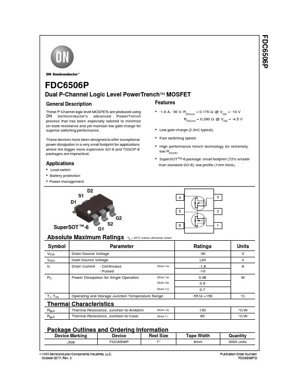
Datasheet4U Logo Datasheet4U.com

FDC6506P - Dual P-Channel MOSFET

Key Features

  • These P-Channel logic level MOSFETs are produced using ON Semiconductor's advanced PowerTrench process that has been especially tailored to minimize on-state resistance and yet maintain low gate charge for superior switching performance.
  • -1.8 A, -30 V. RDS(on) = 0.170 Ω @ VGS = -10 V RDS(on) = 0.280 Ω @ VGS = -4.5 V.
  • Low gate charge (2.3nC typical). These devices have been designed to offer exceptional power dissipation in a very small footprint for.

📥 Download Datasheet

Datasheet Details

Part number FDC6506P
Manufacturer onsemi
File Size 165.13 KB
Description Dual P-Channel MOSFET
Datasheet download datasheet FDC6506P Datasheet

Full PDF Text Transcription (Reference)

The following content is an automatically extracted verbatim text from the original manufacturer datasheet and is provided for reference purposes only.

View original datasheet text
FDC6506P FDC6506P Dual P-Channel Logic Level PowerTrench™ MOSFET General Description Features These P-Channel logic level MOSFETs are produced using ON Semiconductor's advanced PowerTrench process that has been especially tailored to minimize on-state resistance and yet maintain low gate charge for superior switching performance. • -1.8 A, -30 V. RDS(on) = 0.170 Ω @ VGS = -10 V RDS(on) = 0.280 Ω @ VGS = -4.5 V • Low gate charge (2.3nC typical). These devices have been designed to offer exceptional power dissipation in a very small footprint for applications where the bigger more expensive SO-8 and TSSOP-8 packages are impractical. Applications • Load switch • Battery protection • Power management • Fast switching speed.