FDD3510H
FDD3510H is Dual N & P-Channel Power MOSFET manufactured by onsemi.
Features
Q1: N-Channel
- Max r DS(on) = 80mΩ at VGS = 10V, ID = 4.3A
- Max r DS(on) = 88mΩ at VGS = 6V, ID = 4.1A
Q2: P-Channel
- Max r DS(on) = 190mΩ at VGS = -10V, ID = -2.8A
- Max r DS(on) = 224mΩ at VGS = -4.5V, ID = -2.6A
- 100% UIL Tested
- Ro HS pliant
General Description
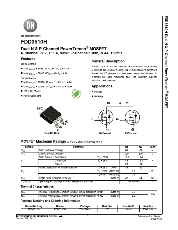
These dual N and P- Channel enhancement mode Power MOSFETs are produced using ON Semiconductor’s advanced Power Trench® process that has been especially tailored to minimize on -state resistance and yet maintain superior switching performance.
Applications
- Inverter
- H-Bridge
D1/D2
D1
D2
G2 S2
G1 S1
Dual DPAK 4L
G1
G2
S1 N-Channel
S2 P-Channel
MOSFET Maximum Ratings TC = 25°C unless otherwise noted
Symbol VDS VGS ID
Parameter Drain to Source Voltage Gate to Source Voltage Drain Current
- Continuous
- Continuous
- Pulsed Power Dissipation for Single Operation
EAS TJ, TSTG
Single Pulse Avalanche Energy Operating and Storage Junction Temperature Range
Thermal Characteristics
TC = 25°C TA = 25°C
TC = 25°C (Note 1) TA = 25°C (Note 1a) TA = 25°C (Note 1b)
(Note...