FDMS3660S
FDMS3660S is Asymmetric Dual N-Channel MOSFET manufactured by onsemi.
PowerTrench) Power Stage
Asymmetric Dual N- Channel MOSFET
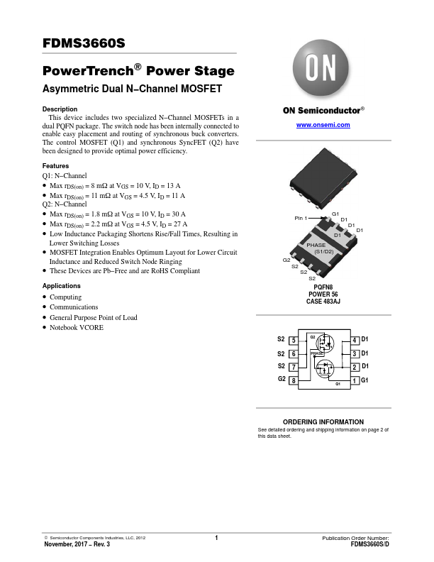
Description This device includes two specialized N- Channel MOSFETs in a dual PQFN package. The switch node has been internally connected to enable easy placement and routing of synchronous buck converters. The control MOSFET (Q1) and synchronous SyncFET (Q2) have been designed to provide optimal power efficiency.
Features
Q1: N- Channel
- Max rDS(on) = 8 mW at VGS = 10 V, ID = 13 A
- Max rDS(on) = 11 mW at VGS = 4.5 V, ID = 11 A
Q2: N- Channel
- Max rDS(on) = 1.8 mW at VGS = 10 V, ID = 30 A
- Max rDS(on) = 2.2 mW at VGS = 4.5 V, ID = 27 A
- Low Inductance Packaging Shortens Rise/Fall Times, Resulting in
Lower Switching...