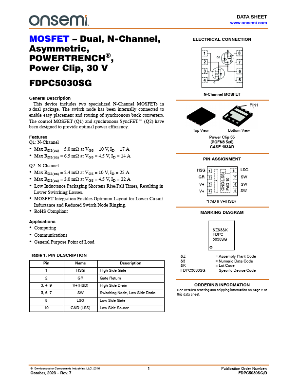
FDPC5030SG Description
This device includes two specialized N-Channel MOSFETs in a dual package. The switch node has been internally connected to enable easy placement and routing of synchronous buck converters. The control MOSFET (Q1) and synchronous SyncFETt (Q2) have been designed to provide optimal power efficiency.
FDPC5030SG Key Features
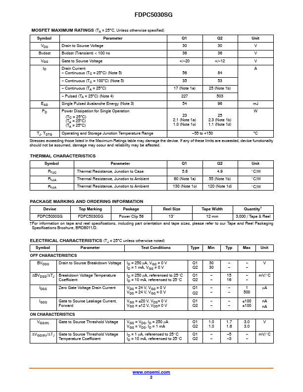
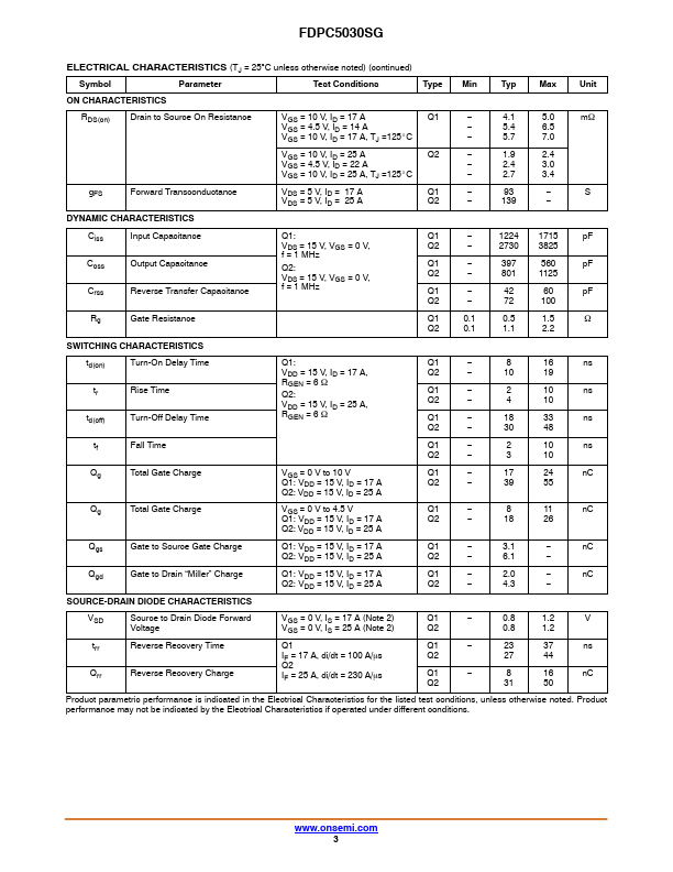
- Max RDS(on) = 5.0 mW at VGS = 10 V, ID = 17 A
- Max RDS(on) = 6.5 mW at VGS = 4.5 V, ID = 14 A
- Max RDS(on) = 2.4 mW at VGS = 10 V, ID = 25 A
- Max RDS(on) = 3.0 mW at VGS = 4.5 V, ID = 22 A
- MOSFET Integration Enables Optimum Layout for Lower Circuit
- RoHS pliant