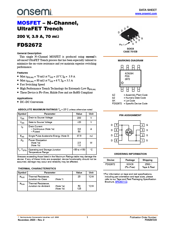
FDS2672
FDS2672 is N-Channel MOSFET manufactured by onsemi.
scription This single N- Channel MOSFET is produced using onsemi’s advanced UItra FET Trench process that has been especially tailored to minimize the on- state resistance and yet maintain superior switching performance.
Features
- Max r DS(on) = 70 m W at VGS = 10 V, ID = 3.9 A
- Max r DS(on) = 80 m W at VGS = 6 V, ID = 3.5 A
- Fast Switching Speed
- High Performance Trench Technology for Extremely Low RDS(on)
- These Device is Pb- Free, Halide Free and are Ro HS pliant
Applications
- DC- DC Conversion
ABSOLUTE MAXIMUM RATINGS TA = 25°C unless otherwise noted
Symbol
Parameter
Value
Unit
VDS Drain to Source Voltage
VGS Gate to Source Voltage
Drain Current
- Continuous (Note 1a)
- Pulsed
±20
EAS Single Pulse Avalanche Energy (Note 3)
37.5 m J
PD Power Dissipation (Note 1a) (Note 1b)
TJ, TSTG Operating and Storage Junction Temperature Range
- 55 to +150 _C
Stresses exceeding those listed in the Maximum Ratings table may damage the device. If any of these limits are exceeded, device functionality should not be assumed, damage may occur and reliability may be affected.
THERMAL CHARACTERISTICS
Symbol
Parameter
RθJC Thermal Resistance, Junction- to-...