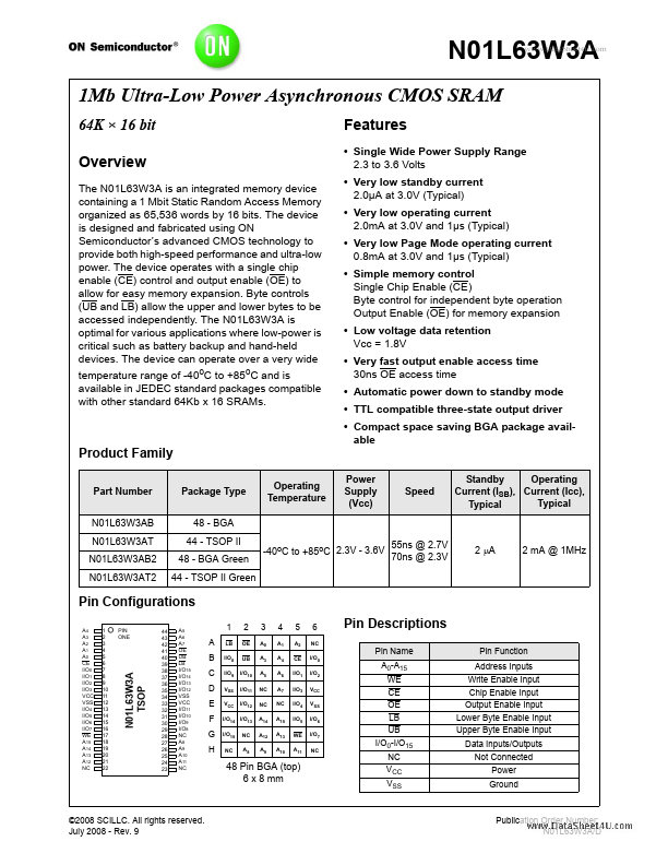
Datasheet Summary
1Mb Ultra-Low Power Asynchronous CMOS SRAM
64K × 16 bit Overview
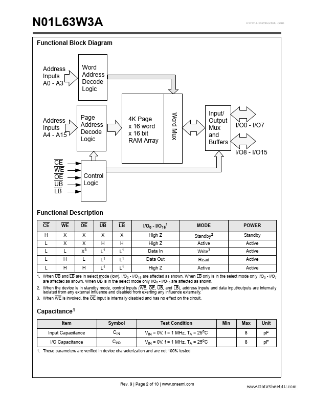
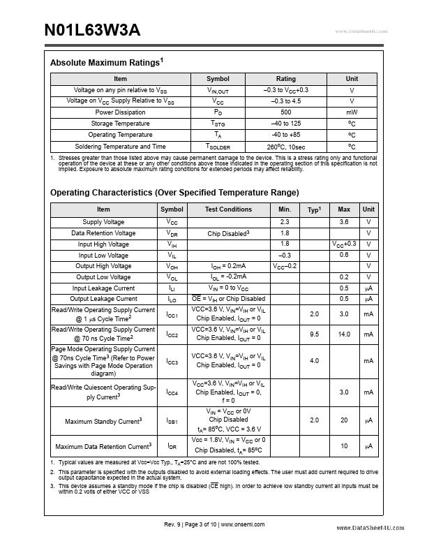
The N01L63W3A is an integrated memory device containing a 1 Mbit Static Random Access Memory organized as 65,536 words by 16 bits. The device is designed and fabricated using ON Semiconductor’s advanced CMOS technology to provide both high-speed performance and ultra-low power. The device operates with a single chip enable (CE) control and output enable (OE) to allow for easy memory expansion. Byte controls (UB and LB) allow the upper and lower bytes to be accessed independently. The N01L63W3A is optimal for various applications where low-power is critical such as battery backup and hand-held devices. The device can...