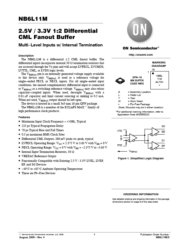
NB6L11M Key Features
- Maximum Input Clock Frequency > 4 GHz, Typical
- 225 ps Typical Propagation Delay
- 70 ps Typical Rise and Fall Times
- 0.5 ps maximum RMS Clock Jitter
- Differential CML Outputs, 380 mV peak-to-peak, typical
- LVPECL Operating Range: VCC = 2.375 V to 3.63 V with VEE = 0 V
- NECL Operating Range: VCC = 0 V with VEE = -2.375 V to -3.63 V
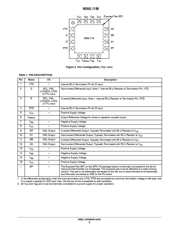
- Internal Input Termination Resistors, 50 W
- VREFAC Reference Output
- Functionally patible with Existing 2.5 V / 3.3V LVEL, LVEP