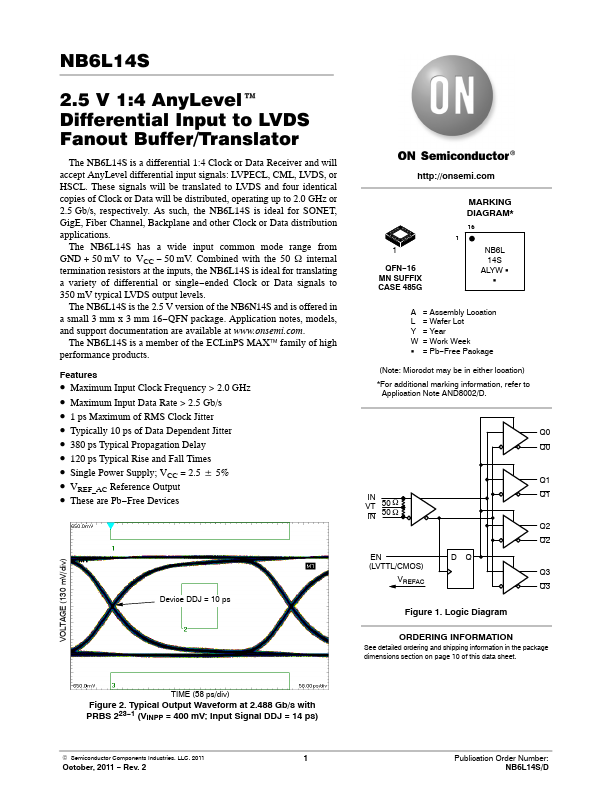
NB6L14S Key Features
- Maximum Input Clock Frequency > 2.0 GHz
- Maximum Input Data Rate > 2.5 Gb/s
- 1 ps Maximum of RMS Clock Jitter
- Typically 10 ps of Data Dependent Jitter
- 380 ps Typical Propagation Delay
- 120 ps Typical Rise and Fall Times
- Single Power Supply; VCC = 2.5 $ 5%
- VREF_AC Reference Output
- These are Pb-Free Devices
- For additional marking information, refer to Application Note AND8002/D