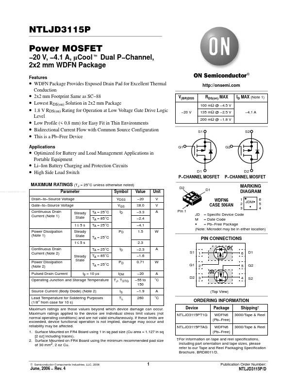
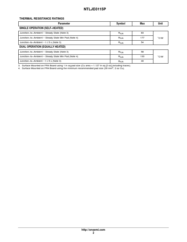
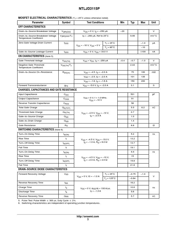
WDFN Package Provides Exposed Drain Pad for Excellent Thermal.
Conduction 2x2 mm Footprint Same as SC.
88 Lowest RDS(on) Solution in 2x2 mm Package 1.8 V RDS(on) Rating for Operation at Low Voltage Gate Drive Logic Level Low Profile (< 0.8 mm) for Easy Fit in Thin Environments Bidirectional Current Flow with Common Source Configuration Thi.
Full PDF Text Transcription for NTLJD3115P (Reference)
Note: Below is a high-fidelity text extraction (approx. 800 characters) for
NTLJD3115P. For precise diagrams, and layout, please refer to the original PDF.
NTLJD3115P Power MOSFET Features −20 V, −4.1 A, mCoolt Dual P−Channel, 2x2 mm WDFN Package • WDFN Package Provides Exposed Drain Pad for Excellent Thermal • • • • • • Con...
View more extracted text
ckage Provides Exposed Drain Pad for Excellent Thermal • • • • • • Conduction 2x2 mm Footprint Same as SC−88 Lowest RDS(on) Solution in 2x2 mm Package 1.8 V RDS(on) Rating for Operation at Low Voltage Gate Drive Logic Level Low Profile (< 0.8 mm) for Easy Fit in Thin Environments Bidirectional Current Flow with Common Source Configuration This is a Pb−Free Device V(BR)DSS http://onsemi.com RDS(on) MAX 100 mW @ −4.5 V −20 V 135 mW @ −2.5 V 200 mW @ −1.8 V S1 S2 −4.