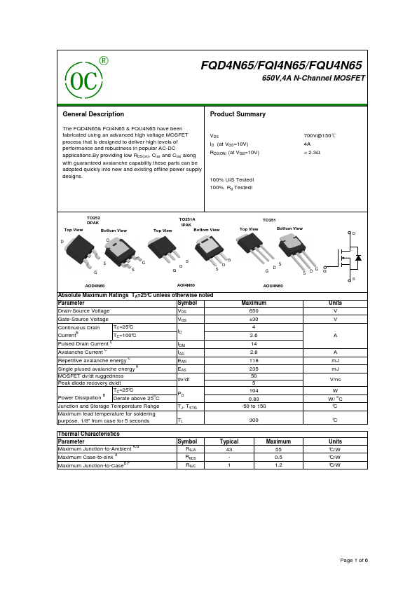
FQD4N65/FQI4N65/FQU4N65
Electrical Characteristics (TJ=25°C unless otherwise noted)
Symbol
Parameter
Conditions
Min Typ Max Units
STATIC PARAMETERS
BVDSS Drain-Source Breakdown Voltage
ID=250µA, VGS=0V, TJ=25°C
ID=250µA, VGS=0V, TJ=150°C
BVDSS
/∆TJ
Zero Gate Voltage Drain Current
ID=250µA, VGS=0V
IDSS Zero Gate Voltage Drain Current
VDS=600V, VGS=0V
VDS=480V, TJ=125°C
IGSS Gate-Body leakage current
VDS=0V, VGS=±30V
VGS(th) Gate Threshold Voltage
VDS=5V, ID=250µA
RDS(ON) Static Drain-Source On-Resistance VGS=10V, ID=2A
gFS Forward Transconductance
VDS=40V, ID=2A
VSD Diode Forward Voltage
IS=1A,VGS=0V
IS Maximum Body-Diode Continuous Current
ISM Maximum Body-Diode Pulsed Current
650
670
V
0.67
V/ oC
1
µA
10
±100 nΑ
3.4 4.1 4.5
V
2.1 2.3
Ω
6S
0.76 1
V
4A
14 A
DYNAMIC PARAMETERS
Ciss Input Capacitance
Coss Output Capacitance
Crss Reverse Transfer Capacitance
Rg Gate resistance
VGS=0V, VDS=25V, f=1MHz
VGS=0V, VDS=0V, f=1MHz
420 528 640
35 53 70
2.5 4.8
7
1.2 2.5 3.8
pF
pF
pF
Ω
SWITCHING PARAMETERS
Qg Total Gate Charge
Qgs Gate Source Charge
VGS=10V, VDS=480V, ID=4A
Qgd Gate Drain Charge
tD(on)
Turn-On DelayTime
tr
tD(off)
Turn-On Rise Time
Turn-Off DelayTime
VGS=10V, VDS=300V, ID=4A,
RG=25Ω
tf Turn-Off Fall Time
trr Body Diode Reverse Recovery Time IF=4A,dI/dt=100A/µs,VDS=100V
Qrr Body Diode Reverse Recovery Charge IF=4A,dI/dt=100A/µs,VDS=100V
9.5 12 14.5 nC
2.8 3.6 4.5 nC
2.2 4.4 6.6 nC
17 ns
26 ns
34 ns
21 ns
150 190 230
1.9 2.4 3
ns
µC
A. The value of R θJA is measured with the device in a still air environment with T A =25°C.
B. The power dissipation PD is based on TJ(MAX)=150°C in a TO252 package, using junction-to-case thermal resistance, and is more useful in
setting the upper dissipation limit for cases where additional heatsinking is used.
C. Repetitive rating, pulse width limited by junction temperature TJ(MAX)=150°C.
D. The R θJA is the sum of the thermal impedance from junction to case R θJC and case to ambient.
E. The static characteristics in Figures 1 to 6 are obtained using <300 µs pulses, duty cycle 0.5% max.
F. These curves are based on the junction-to-case thermal impedance which is measured with the device mounted to a large heatsink, assuming a
maximum junction temperature of TJ(MAX)=150°C.
G.These tests are performed with the device mounted on 1 in2 FR-4 board with 2oz. Copper, in a still air environment with TA=25°C.
H. L=60mH, IAS=2.8A, VDD=150V, RG=10Ω, Starting TJ=25°C
Page 2 of 6