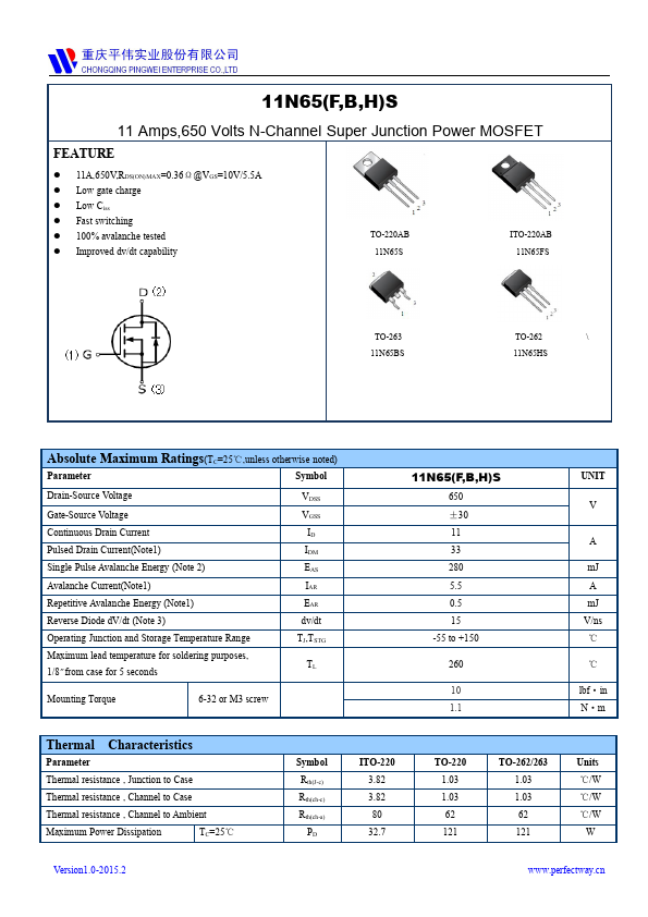
Electrical Characteristics (Tc=25℃,unless otherwise noted)
Parameter
Symbol
Off Characteristics
Drain-Source Breakdown Voltage
BVDSS
Breakdown Temperature Coefficient
ΔBVDSS
/ΔTJ
Zero Gate Voltage Drain Current
IDSS
Gate-Body Leakage Current,Forward
IGSSF
Gate-Body Leakage Current,Reverse
IGSSR
On Characteristics
Gate-Source Threshold Voltage
VGS(th)
Drain-Source On-State Resistance
RDS(on)
Dynamic Characteristics
Input Capacitance
Ciss
Output Capacitance
Coss
Reverse Transfer Capacitance
Crss
Test Conditions
VGS=0V,ID=250uA
Reference to 25℃,
ID=250uA
VDS=650V,VGS=0V
VGS=30V,VDS=0V
VGS=-30V,VDS=0V
VDS=VGS,ID=250uA
VGS=10V,ID=5.5A
VDS=50V,VGS=0V,
f=1.0MHZ
Switching Characteristics
Turn-On Delay Time
td(on)
VDD=380V,ID=5.5A,
Turn-On Rise Time
Turn-Off Delay Time
tr
td(off)
RG=6.8Ω
(Note4,5)
Turn-Off Fall Time
tf
Total Gate Charge
Qg
VDS=480V,ID=11A,
Gate-Source Charge
Qgs
VGS=10V, (Note4,5)
Gate-Drain Charge
Qgd
Drain-Source Body Diode Charcteristics and Maximum Ratings
Continuous Diode Forward Current
IS
Pulsed Diode Forward Current
ISM
Diode Forward Voltage
VSD
IS=11A,VGS=0V
Reverse Recovery Time
trr
VGS=0V,IS=11A,
Reverse Recovery Charge
Qrr
dIF/dt=100A/us, (Note4)
Notes
1. Repetitive Rating:pulse width limited by maximum junction temperature.
2. VDD=50V,L=4.6mH,Rg=25Ω,IAS=11A ,starling TJ=25℃.
3. ISD≤ID,dI/dt=200A/us,VDD≤BVDSS,starting TJ=25℃.
4. Pulse width≤300us;duty cycle≤2%.
5. Repetitive rating; pulse width limited by maximum junction temperature.
Min Typ Max Units
600 -
- 0.6
-
-
-
-
-
-
-
V
- V/℃
1
μA
1
μA
-1
μA
2
-
4
V
- 0.30 0.36
Ω
- 1030 -
pF
-
87
-
pF
-
4.5
-
pF
-
9
-
ns
-
4
-
ns
-
40
-
ns
-
4.5
-
ns
-
23
-
nC
-
5.7
-
nC
-
8.0
-
nC
-
-
11
A
-
-
33
A
-
-
1.3
V
- 245 -
ns
-
2.4
-
μC
Version1.0-2015.2
www.perfectway.cn