2SA1619A Overview
Key Specifications
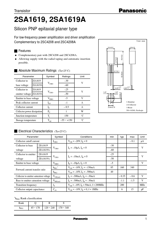
Package: TO-226-3
Mount Type: Through Hole
Key Features
- IB Collector power dissipation PC (W) –600 –500 –400 –300 –200
| Part | 2SA1619A |
|---|---|
| Description | Silicon PNP epitaxial planer type Transistor |
| Category | Transistor |
| Manufacturer | Panasonic |
| Size | 47.26 KB |
Package: TO-226-3
Mount Type: Through Hole
| Seller | Inventory | Price Breaks | Buy |
|---|---|---|---|
| Component Stockers USA | 292 | 1+ : 99.99 USD | View Offer |
| Part Number | Manufacturer | Description |
|---|---|---|
| A1615 | NEC | 2SA1615 |
| 2SA1617 | Hitachi Semiconductor | Silicon PNP Epitaxial Transistor |
| 2SA1611 | Galaxy Microelectronics | PNP Silicon Transistor |
| 2SA1611 | NEC | AUDIO FREQUENCY GENERAL PURPOSE AMPLIFIER PNP SILICON EPITAXIAL TRANSISTOR |
| 2SA1611 | JCET | PNP Transistor |