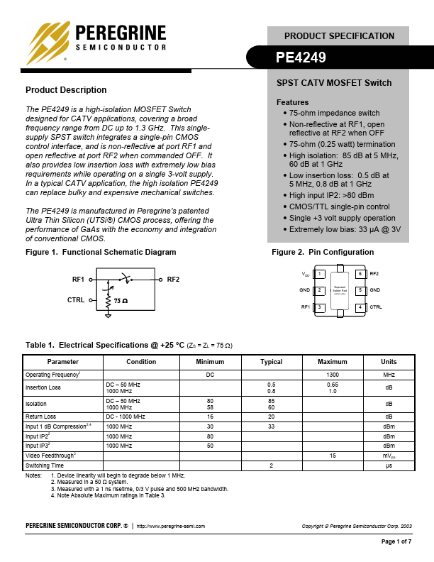
Table 2. Pin Descriptions
Pin Pin
No. Name
Description
1 VDD Nominal 3 V supply connection.1
2
GND
Ground connection. 3
3 RF1 RF port. 2
CMOS or TTL logic level:
4 CTRL
High = RF1 to RF2 signal path
Low = RF1 isolated from RF2
5 GND Ground connection. 3
6 RF2 RF port. 2
Notes: 1. A bypass capacitor should be placed as close as possible to
the pin.
2. Both RF pins must be DC blocked by an external capacitor
or held at 0 VDC.
3. The exposed pad must be soldered to the ground plane for
proper switch performance.
Table 3. Absolute Maximum Ratings
Symbol
VDD
VI
TST
TOP
PIN
VESD
Parameter/Condition
Power supply voltage
Voltage on CTRL input
Storage temperature
Operating temperature
Input power (50Ω),
CTRL=1/CTRL=0
ESD voltage
(Human Body Model)
Min Max Unit
-0.3 4.0
V
-0.3 5.5
V
-65 150
-40 85
°C
°C
33/24 dBm
500 V
Table 4. DC Electrical Specifications @ 25 °C
Parameter
VDD Power Supply
IDD Power Supply Current
(VDD = 3V, VCNTL = 3V)
Control Voltage High
Control Voltage Low
Min
2.7
70% VDD
0
Typ
3.0
33
Max
3.3
40
5
30% VDD
Unit
V
µA
V
V
Copyright Peregrine Semiconductor Corp. 2003
Page 2 of 7
PE4249
Product Specification
Electrostatic Discharge (ESD) Precautions
When handling this UTSi device, observe the same
precautions that you would use with other ESD-
sensitive devices. Although this device contains
circuitry to protect it from damage due to ESD,
precautions should be taken to avoid exceeding the
rating specified.
Latch-Up Avoidance
Unlike conventional CMOS devices, UTSi CMOS
devices are immune to latch-up.
Device Description
The PE4249 high isolation SPST CATV Switch is
designed to support CATV applications such as
premium channel service connect/disconnect switch
blocks. This function is typically performed by bulky
and expensive mechanical switches. The high
isolation characteristics (60 dB at 1 GHz, 85 dB at 5
MHz), high compression point, and an integrated 75
Ω (0.25 watt) input termination make the PE4249 an
ideal, low cost solution.
Figure 3. Typical Application Block Diagram
CATVin
2-way
Splitter
Premium
Channel
Filter
PE4249
PE4249
CATVout
Table 5. Truth Table
Control Voltage (CTRL)
High1
Low
Signal Path (RF1 to RF2)
ON
OFF
Notes: 1. CTRL accepts both CMOS and TTL voltage leads.
The control logic input pin (CTRL) is typically driven
by a 3-volt CMOS logic level signal, and has a
threshold of 50% of VDD. For flexibility to support
systems that have 5-volt control logic drivers, the
control logic input has been designed to handle a 5-
volt logic HIGH signal. (A minimal current will be
sourced out of the VDD pin when the control logic
input voltage level exceeds VDD.)
File No. 70/0110~00C | UTSi CMOS RFIC SOLUTIONS