Datasheet4U Logo Datasheet4U.com

PLL620-08 - (PLL620-05/06/07/08/09) Low Phase Noise XO

This page provides the datasheet information for the PLL620-08, a member of the PLL620-05 (PLL620-05/06/07/08/09) Low Phase Noise XO family.

Datasheet Summary

Description

GND GND GND BLOCK DIAGRAM SEL ^: Internal pull-up : PLL620-06 pin 12 is output drive select (DRIVSEL) (0 for High Drive CMOS, 1 for Standard Drive CMOS) OE Q Q X+ X- Oscillator Amplifier PLL (Phase Locked Loop) OUTPUT ENABLE LOGICAL LEVELS Part # PLL620-08 PLL620-05 PLL620-06 PLL620-

Features

  • h PIN.

📥 Download Datasheet

Datasheet preview – PLL620-08

Datasheet Details

Part number PLL620-08
Manufacturer PhaseLink
File Size 180.03 KB
Description (PLL620-05/06/07/08/09) Low Phase Noise XO
Datasheet download datasheet PLL620-08 Datasheet
Additional preview pages of the PLL620-08 datasheet.
Other Datasheets by PhaseLink

Full PDF Text Transcription

Click to expand full text
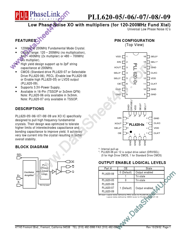
m PLL620-05/-06/-07/-08/-09 o c . XO with multipliers (for 120-200MHz Fund Xtal) Low Phase Noise U Universal Low Phase Noise IC’s 4 t e e FEATURES h PIN CONFIGURATION S (Top View) a200MHz Fundamental Mode Crystal. • 120MHz to t • Output a range: 120 – 200MHz (no multiplication), D 240 – 400MHz (2x multiplier) or 480 – 700MHz . (4x multiplier). w •w High yield design support up to 2pF string at 200MHz. w• capacitance CMOS (Standard drive PLL620-07 or Selectable VDD 1 2 3 4 5 6 7 8 16 15 14 13 12 11 10 9 SEL0^ SEL1^ GND XIN • • GND/ DRIVSEL* Drive PLL620-06), PECL (Enable low PLL620-08 or Enable high PLL620-05) or LVDS output (PLL620-09). Supports 3.3V-Power Supply. Available in 16-Pin (TSSOP or 3x3mm QFN) Note: PLL620-06 only available in 3x3mm. Note: PLL620-07 only available in TSSOP.
Published: |