Datasheet4U Logo Datasheet4U.com

71V2556S - 3.3V Synchronous SRAMs

Datasheet Summary

Description

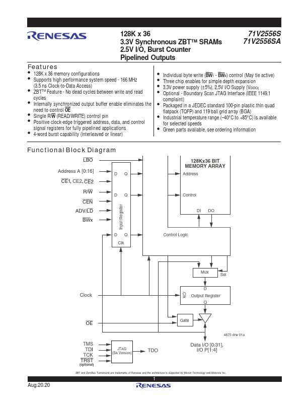
The IDT71V2556 is a 3.3V high-speed 4,718,592-bit (4.5 Megabit) synchronous SRAM.

It is designed to eliminate dead bus cycles when turning the bus around between reads and writes, or writes and reads.

Thus, they have been given the name ZBTTM, or Zero Bus Turnaround.

Features

  • 128K x 36 memory configurations.
  • Supports high performance system speed - 166 MHz (3.5 ns Clock-to-Data Access).
  • ZBTTM Feature - No dead cycles between write and read cycles.
  • Internally synchronized output buffer enable eliminates the need to control OE.
  • Single R/W (READ/WRITE) control pin.
  • Positive clock-edge triggered address, data, and control signal registers for fully pipelined.

📥 Download Datasheet

Datasheet preview – 71V2556S

Datasheet Details

Part number 71V2556S
Manufacturer Renesas
File Size 300.74 KB
Description 3.3V Synchronous SRAMs
Datasheet download datasheet 71V2556S Datasheet
Additional preview pages of the 71V2556S datasheet.
Other Datasheets by Renesas

Full PDF Text Transcription

Click to expand full text
128K x 36 3.3V Synchronous ZBT™ SRAMs 2.5V I/O, Burst Counter Pipelined Outputs 71V2556S 71V2556SA Features ◆ 128K x 36 memory configurations ◆ Supports high performance system speed - 166 MHz (3.5 ns Clock-to-Data Access) ◆ ZBTTM Feature - No dead cycles between write and read cycles ◆ Internally synchronized output buffer enable eliminates the need to control OE ◆ Single R/W (READ/WRITE) control pin ◆ Positive clock-edge triggered address, data, and control signal registers for fully pipelined applications ◆ 4-word burst capability (interleaved or linear) ◆ Individual byte write (BW1 - BW4) control (May tie active) ◆ Three chip enables for simple depth expansion ◆ 3.3V power supply (±5%), 2.5V I/O Supply (VDDQ) ◆ Optional - Boundary Scan JTAG Interface (IEEE 1149.
Published: |