logo

894D115I-01 Datasheet, Renesas

894D115I-01 Datasheet, Renesas

894D115I-01

datasheet Download (Size : 390.76KB)

894D115I-01 Datasheet

894D115I-01 recovery

clock/data recovery.

894D115I-01

datasheet Download (Size : 390.76KB)

894D115I-01 Datasheet

894D115I-01 Features and benefits


* Clock recovery for STM-4 (OC-12/STS-12) and STM-1 (OC-3/STS-3)
* Input: NRZ data (622.08 or 155.52 Mbit/s)
* Output: clock signal (622.08MHz or 155.52MHz) a.

894D115I-01 Application

BYPASS set to logic HIGH state is used during factory test. In BYPASS mode (BYPASS and STS12 are at logic HIGH state), .

894D115I-01 Description

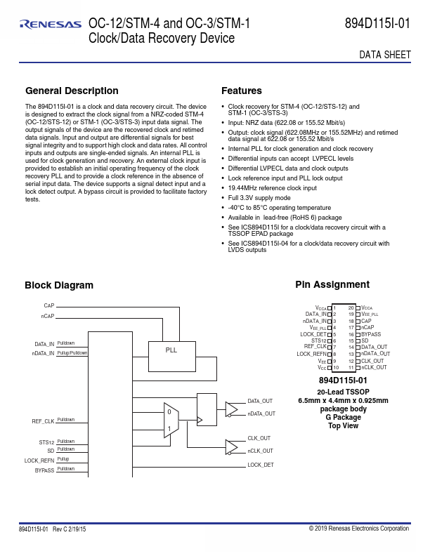
The 894D115I-01 is a clock and data recovery circuit. The device is designed to extract the clock signal from a NRZ-coded STM-4 (OC-12/STS-12) or STM-1 (OC-3/STS-3) input data signal. The output signals of the device are the recovered clock and retim.

Image gallery

894D115I-01 Page 1 894D115I-01 Page 2 894D115I-01 Page 3

TAGS

894D115I-01
Clock
Data
Recovery
Renesas

Manufacturer


Renesas (https://www.renesas.com/)

Related datasheet

894D115I-04

894-2AC1-F-C

894-2AC1-F-S

894-2AC1-F-V

894-2AC2-F-C

894-2AC2-F-S

894-2AC2-F-V

894-2ACA1-F-C

894-2ACA1-F-S

894-2ACA1-F-V

894-2ACA2-F-C

894-2ACA2-F-S

894-2ACA2-F-V

Since 2006. D4U Semicon.   |   Contact Us   |   Privacy Policy   |   Purchase of parts