Datasheet4U Logo Datasheet4U.com

894D115I-04 Datasheet - Renesas

 datasheet Preview Page 1 from Datasheet4u.com

894D115I-04 Clock/Data Recovery

OC-12/STM-4 AND OC-3/STM-1 Clock/Data Recovery Device 894D115I-04 Data Sheet General .
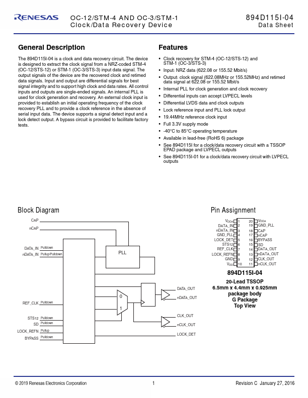
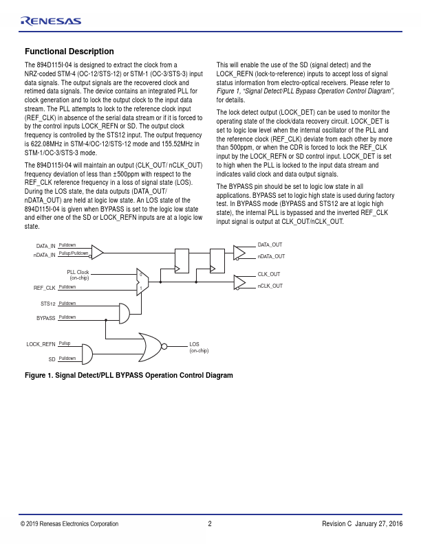
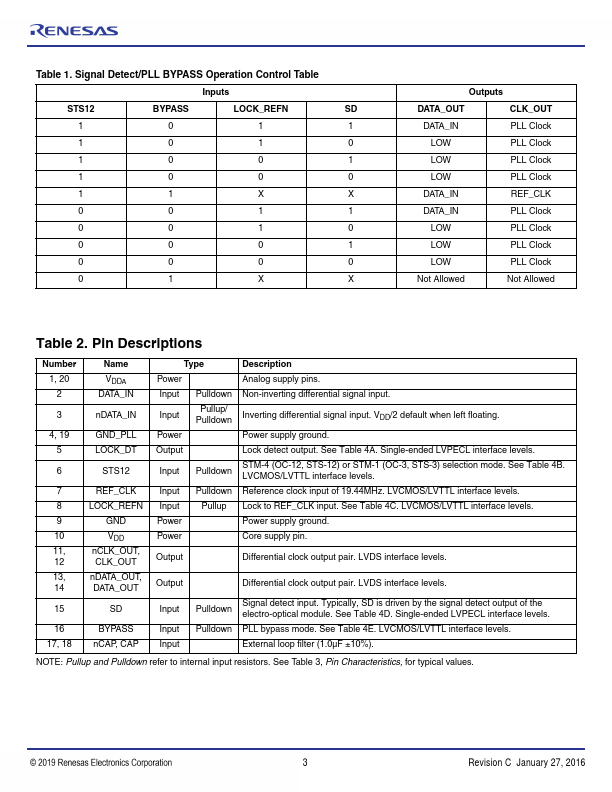
The 894D115I-04 is a clock and data recovery circuit.

894D115I-04-Renesas.pdf

Preview of 894D115I-04 PDF

Datasheet Details

Part number:

894D115I-04

Manufacturer:

Renesas ↗

File Size:

402.23 KB

Description:

Clock/Data Recovery

Features

* Clock recovery for STM-4 (OC-12/STS-12) and STM-1 (OC-3/STS-3)
* Input: NRZ data (622.08 or 155.52 Mbit/s)
* Output: clock signal (622.08MHz or 155.52MHz) and retimed data signal at 622.08 or 155.52 Mbit/s
* Internal PLL for clock generation and clock recovery

Applications

* BYPASS set to logic high state is used during factory test. In BYPASS mode (BYPASS and STS12 are at logic high state), the internal PLL is bypassed and the inverted REF_CLK input signal is output at CLK_OUT/nCLK_OUT. DATA_IN Pulldown nDATA_IN Pullup/Pulldown PLL Clock (on-chip) REF_CLK Pulldown ST

894D115I-04 Distributors

📁 Related Datasheet

📌 All Tags

Renesas 894D115I-04-like datasheet