9DB833 Overview
Description
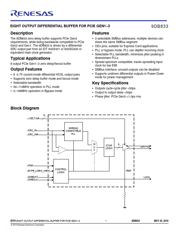
The 9DB833 zero-delay buffer supports PCIe Gen3 requirements, while being backwards compatible to PCIe Gen2 and Gen1. The 9DB833 is driven by a differential SRC output pair from an IDT 932S421 or 932SQ420 or equivalent main clock generator.
Key Features
- 3 selectable SMBus addresses; multiple devices can share the same SMBus segment
- OE# pins; suitable for Express Card applications
- PLL or bypass mode; PLL can dejitter incoming clock
- Selectable PLL bandwidth; minimizes jitter peaking in downstream PLLs
- Spread spectrum compatible; tracks spreading input clock for low EMI
- SMBus interface; unused outputs can be disabled
- Supports undriven differential outputs in Power Down mode for power management Key Specifications
- Outputs cycle-cycle jitter <50ps
- Output to output skew <50ps
- Phase jitter: PCIe Gen3 <1.0ps rms