9QXL2001B
9QXL2001B is PCIe Clock Buffer manufactured by Renesas.
Description
The 9QXL2001B is a 20-output very-low-additive phase jitter fanout buffer for PCIe Gen4, Gen5 and UPI applications. The 9QXL2001B provides two methods to control output enables; standard OE# pins and SMBus enable bits, or a simple 3-wire serial interface that is independent of the SMBus. The OE Control Mode is set via a hardware strap. It offers integrated terminations for 85Ω transmission lines.
PCIe Clocking Architectures
- mon Clocked (CC)
- Independent Reference (IR) with and without spread spectrum
Typical Applications
- Servers, Storage, Networking, Accelerators
Features
- Two Output Enable Control modes:
- Traditional 8 OE# pins allow hardware control of 8 outputs and 20 SMBus bits allow software control of each output
- Simple 3-wire Side-Band Interface allows real-time control of all 20 outputs
- Outputs remain Low/Low when powered up with floating input clock
- Low-Power HCSL (LP-HCSL) outputs:
- Zo = 85Ω outputs eliminate 80 resistors, saving 130mm2 of area
- Power consumption reduced by 50%
- Nine selectable SMBus addresses
- Spread spectrum patible
- 6 × 6 mm dual-row 80-VFQFPN
Key Specifications
- Output-to-output skew: < 50ps
- Additive phase jitter: DB2000Q < 25fs rms
- Additive phase jitter: PCIe Gen4 < 40fs rms
- Additive phase jitter: PCIe Gen5 < 20fs rms
Output Features
20 Low-Power HCSL (LP-HCSL) 85Ω output pairs
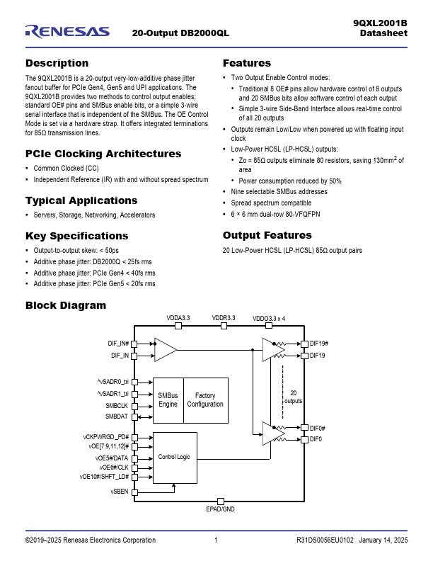
Block Diagram
VDDA3.3
VDDR3.3
VDDO3.3 x 4
DIF_IN# DIF_IN
DIF19# DIF19
^v SADR0_tri ^v SADR1_tri
SMBCLK SMBDAT v CKPWRGD _PD# v OE[7:9,11,12]# v OE5#/DATA v OE6#/CLK v OE10#/SHFT_LD# v SBEN
SMBus Factory Engine Configuration
Control Logic
EPAD/GND
20 outputs
DIF0# DIF0
©2019- 2025 Renesas Electronics...