9QXL2001C
9QXL2001C is PCIe Clock Buffer manufactured by Renesas.
Description
The 9QXL2001C is an enhanced-performance 9QXL2001B with ultra-low-additive phase jitter for PCIe Gen5, Gen6 and UPI applications. The 9QXL2001C also reduces propagation delay by approximately 50% with respect to the 9QXL2001B.
PCIe Clocking Architectures
- mon Clocked (CC)
- Independent Reference (IR)
- SRNS, SRIS
Applications
- Servers, Storage, Networking, Accelerators
- Key Specifications
- Output-to-output skew: < 50ps
- PCIe Gen5 additive phase jitter: 6fs RMS
- PCIe Gen6 additive phase jitter: 4fs RMS
- DB2000Q additive phase jitter: 10fs RMS
- 12k Hz- 20MHz additive jitter: 23fs RMS at
156.25MHz
- Propagation delay: 1.4ns typical
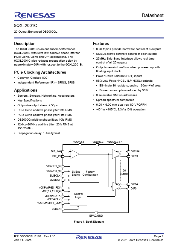
VDDA3.3
Features
- 8 OE# pins provide hardware control of 8 outputs
- SMBus allows software control of each output
- 25MHz Side-Band Interface allows real-time control of all 20 outputs
- Outputs remain Low/Low when powered up with floating input clock
- Power Down Tolerant (PDT) inputs
- 85Ω Low-Power HCSL (LP-HCSL) outputs:
- Eliminate 80 resistors, saving 130mm2 of area
- Power consumption reduced by 50%
- 9 selectable SMBus addresses
- Spread spectrum patible
- 6.00 × 6.00 mm dual-row 80-VFQFPN
- -40° to +105°C, 3.3V ±10% operation
VDDR3.3 VDDO3.3 x 4
DIF_IN# DIF_IN
DIF19# DIF19
^v SADR0_tri ^v SADR1_tri
SMBCLK SMBDAT v CKPWRGD_PD# v OE[7:9,11,12]# v OE5#/DATA v OE6#/CLK v OE10#/SHFT_LD# v SBEN
SMBus Factory Engine Configuration
Control Logic
EPAD/GND Figure 1. Bock Diagram
20 outputs
DIF0#...