Datasheet Summary
3.3V PCIe® Gen1- 5 and UPI Clock Generator Family
9SQL4952/9SQL4954/ 9SQL4958 Datasheet
Description
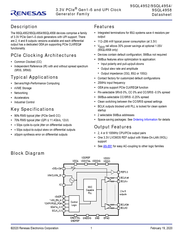
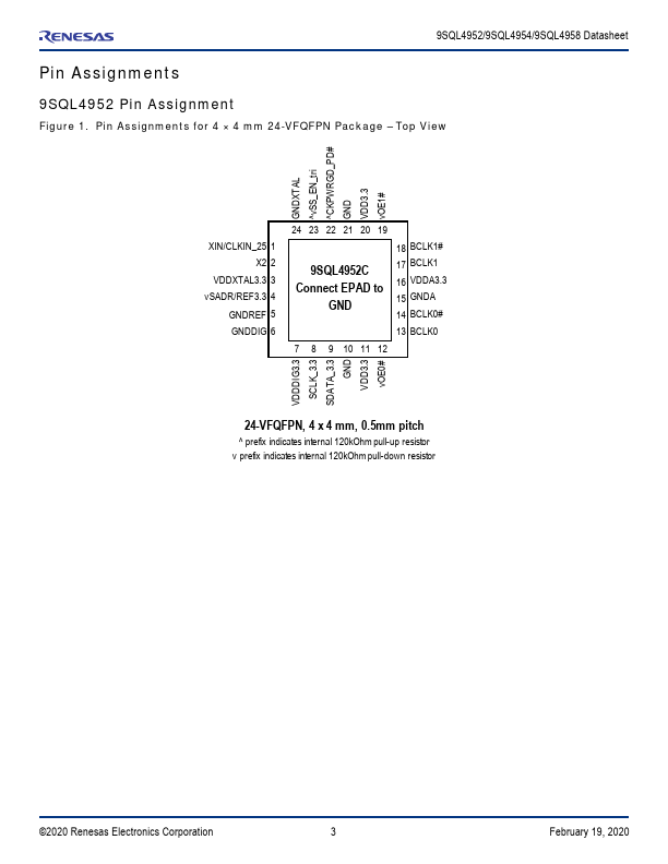
The 9SQL4952/9SQL4954/9SQL4958 devices prise a family of 3.3V PCIe Gen1- 5 clock generators with UPI support. There are 2, 4 and 8 outputs versions available and each differential output has a dedicated OE# pin supporting PCIe CLKREQ# functionality.
PCIe Clocking Architectures
- mon Clocked (CC)
- Independent Reference (IR) with and without spread spectrum
(SRIS, SRNS)
Typical Applications
- Servers/High-Performance puting
- nVME Storage
- Networking
- Accelerators
- Industrial Control
Key Specifications
- 90fs RMS typical jitter (PCIe Gen5 CC)
- 70fs RMS typical jitter (QPI ≤...