HD74CDCV857 Overview
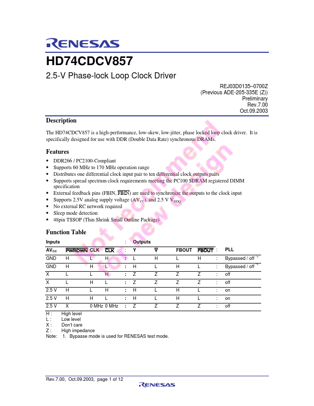
REJ03D0135 0700Z (Previous ADE-205-335E (Z)) Preliminary Rev.7.00 Oct.09.2003 The HD74CDCV857 is a high-performance, low-skew, low-jitter, phase locked loop clock driver. It is specifically designed for use with DDR (Double Data Rate) synchronous DRAMs.
HD74CDCV857 Key Features
- DDR266 / PC2100-pliant
- Supports 60 MHz to 170 MHz operation range
- Distributes one differential clock input pair to ten differential clock outputs pairs
- Supports spread spectrum clock requirements meeting the PC100 SDRAM registered DIMM
- External feedback pins (FBIN, FBIN) are used to synchronize the outputs to the clock input
- Supports 2.5V analog supply voltage (AVCC), and 2.5 V VDDQ
- No external RC network required
- Sleep mode detection
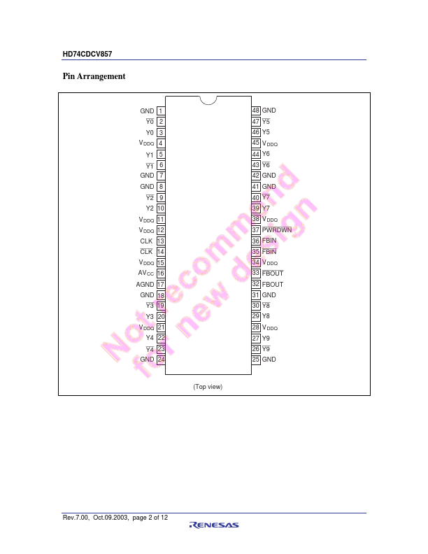
- 48pin TSSOP (Thin Shrink Small Outline Package)