ICS650-27
ICS650-27 is NETWORKING CLOCK SOURCE manufactured by Renesas.
NETWORKING CLOCK SOURCE
Description
The ICS650-27 is a low cost, low jitter, high performance clock synthesizer for networking applications. Using analog Phase-Locked Loop (PLL) techniques, the device accepts a 12.5 MHz or 25 MHz clock or fundamental mode crystal input to produce multiple output clocks for networking chips, PCI devices, SDRAM, and ASICs. The ICS650-27 outputs all have zero ppm synthesis error.
The ICS650-27 is pin patible and functionally equivalent to the ICS650-07. It is a performance upgrade and is remended for all new 3.3V designs.
See the MK74CB214, ICS551, and ICS552-01 for non-PLL buffer devices which produce multiple low-skew copies of these output clocks.
See the ICS570, ICS9112-16/17/18 for zero delay buffers that can synchronize outputs and other needed clocks.
Features
- Packaged in 20-pin (150 mil) SSOP (QSOP)
- Pb (lead) free package, Ro HS pliant
- 12.5 MHz or 25 MHz fundamental crystal or clock input
- Six output clocks with selectable frequencies
- SDRAM frequencies of 67, 83, 100, and 133 MHz
- Buffered crystal reference output
- Zero ppm synthesis error in all clocks
- Ideal for PMC-Sierra’s ATM switch chips
- Full CMOS output swing with 25 m A output drive capability at TTL levels
- Advanced, low-power, sub-micron CMOS process
- Operating voltage of 3.3 V
- Industrial temperature only
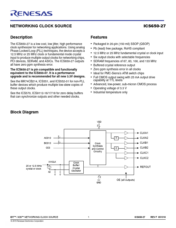
Block Diagram
ACS1:0 BCS1:0
2 2
25 or 12.5 MHz cyrstal or clock
X1/ICLK X2
VDD 2
Clock Buffer/ Crystal Oscillator
Clock Synthesis and Control Circuitry
2 GND
CLKA1 /2 CLKA2
CLKB1 /2...