ICS8305I-02
ICS8305I-02 is LVCMOS-to-LVCMOS Fanout Buffer manufactured by Renesas.
Description
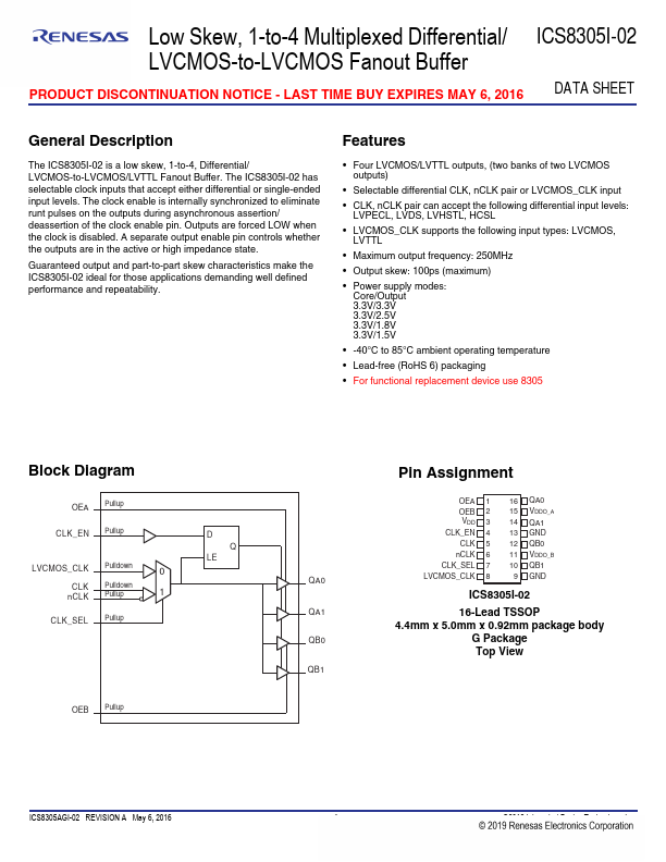
The ICS8305I-02 is a low skew, 1-to-4, Differential/ LVCMOS-to-LVCMOS/LVTTL Fanout Buffer. The ICS8305I-02 has selectable clock inputs that accept either differential or single-ended input levels. The clock enable is internally synchronized to eliminate runt pulses on the outputs during asynchronous assertion/ deassertion of the clock enable pin. Outputs are forced LOW when the clock is disabled. A separate output enable pin controls whether the outputs are in the active or high impedance state.
Guaranteed output and part-to-part skew characteristics make the ICS8305I-02 ideal for those applications demanding well defined performance and repeatability.
Features
- Four LVCMOS/LVTTL outputs, (two banks of two LVCMOS outputs)
- Selectable differential CLK, n CLK pair or LVCMOS_CLK input
- CLK, n CLK pair can accept the following differential input levels:
LVPECL, LVDS, LVHSTL, HCSL
- LVCMOS_CLK supports the following input types: LVCMOS,
LVTTL
- Maximum output frequency: 250MHz
- Output skew: 100ps (maximum)
- Power supply modes:
Core/Output 3.3V/3.3V 3.3V/2.5V 3.3V/1.8V 3.3V/1.5V
- -40°C to 85°C ambient operating temperature
- Lead-free (Ro HS 6) packaging
- For functional replacement device use 8305
Block Diagram
OEA Pullup CLK_EN Pullup
LVCMOS_CLK Pulldown
CLK n CLK
Pulldown Pullup
CLK_SEL Pullup
OEB Pullup
QA0 QA1 QB0 QB1
Pin Assignment
OEA 1 OEB 2 VDD 3 CLK_EN 4 CLK 5 n CLK 6 CLK_SEL 7 LVCMOS_CLK 8
16 QA0 15 VDDO_A 14 QA1 13 GND 12 QB0 11 VDDO_B 10 QB1
9 GND
16-Lead TSSOP 4.4mm x 5.0mm x 0.92mm package body
G Package Top View
ICS8305AGI-02 REVISION A May 6, 2016
©2016 Integrated Device Technology, Inc.
ICS8305I-02 Data Sheet
LOW SKEW, 1-TO-4 MULTIPLEXED DIFFERENTIAL/LVCMOS-TO-LVCMOS FANOUT BUFFER
Table 1. Pin...