ICS91720
ICS91720 is Clock Generator manufactured by Renesas.
Low EMI, Spread Modulating, Clock Generator
Features
:
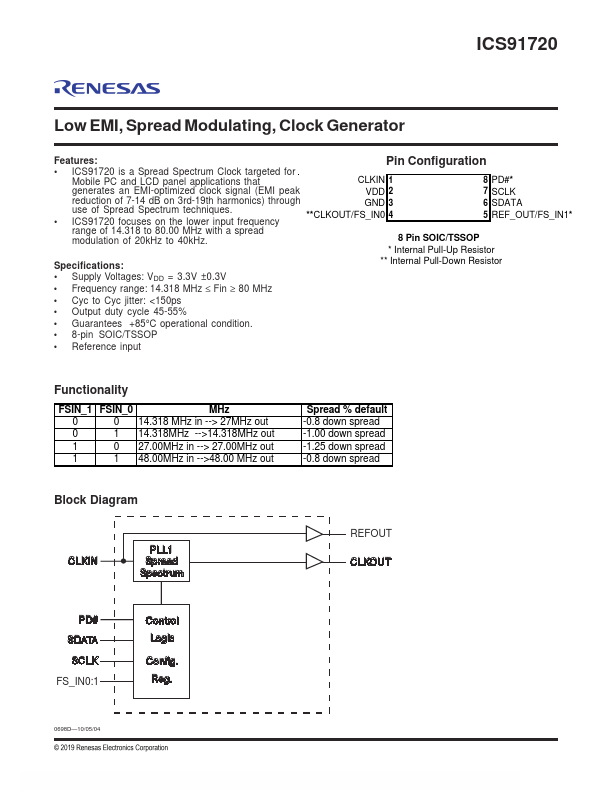
Pin Configuration
- ICS91720 is a Spread Spectrum Clock targeted for Mobile PC and LCD panel applications that
CLKIN 1
8 PD#- generates an EMI-optimized clock signal (EMI peak
VDD 2
7 SCLK reduction of 7-14 d B on 3rd-19th harmonics) through
GND 3 use of Spread Spectrum techniques.
- - CLKOUT/FS_IN0 4
- ICS91720 focuses on the lower input frequency
6 SDATA 5 REF_OUT/FS_IN1- range of 14.318 to 80.00 MHz with a spread modulation of 20k Hz to 40k Hz.
8 Pin SOIC/TSSOP
- Internal Pull-Up Resistor
Specifications:
- - Internal Pull-Down Resistor
- Supply Voltages: VDD = 3.3V ±0.3V
- Frequency range: 14.318 MHz ≤ Fin ≥ 80 MHz
- Cyc to Cyc jitter: <150ps
- Output duty cycle 45-55%
- Guarantees +85°C operational condition.
- 8-pin SOIC/TSSOP
- Reference input
Functionality
FSIN_1 FSIN_0
MHz
0 0 14.318 MHz in --> 27MHz out
0 1 14.318MHz -->14.318MHz out
1 0 27.00MHz in --> 27.00MHz...