Datasheet4U Logo Datasheet4U.com

M6MGB33BS8BWG - CMOS SRAM

Download the M6MGB33BS8BWG datasheet PDF. This datasheet also covers the M6MGT33BS8BWG variant, as both devices belong to the same cmos sram family and are provided as variant models within a single manufacturer datasheet.

Description

The M6MGB/T33BS8BWG is a Stacked Chip Scale Package The M6MGB/T33BS8BWG is suitable for a high performance cellular phone and a mobile PC that are required to be small (S-CSP) that contents 32M-bit Flash memory and 8M-bit mounting area, weight and small power dissipation.

Features

  • Access Time Flash SRAM 70ns (Max. ) 85ns (Max. ) F-VCC =VCC=2.7 ~ 3.0V Ta=-40 ~ 85 °C 66 pin S-CSP Ball pitch 0.80mm Outer-ball:Sn.
  • Ag-Cu Supply Voltage Ambient Temperature Package.

📥 Download Datasheet

Note: The manufacturer provides a single datasheet file (M6MGT33BS8BWG_Renesas.pdf) that lists specifications for multiple related part numbers.

Full PDF Text Transcription (Reference)

The following content is an automatically extracted verbatim text from the original manufacturer datasheet and is provided for reference purposes only.

View original datasheet text
www.DataSheet4U.com Preliminary Notice: This is not a final specification. Some parametric limits are subject to change. Renesas LSIs M6MGB/T33BS8BWG 33,554,432-BIT (2,097,152-WORD BY 16-BIT) CMOS FLASH MEMORY 8,388,608-BIT (524,288-WORD BY 16-BIT) CMOS SRAM Stacked-CSP (Chip Scale Package) &
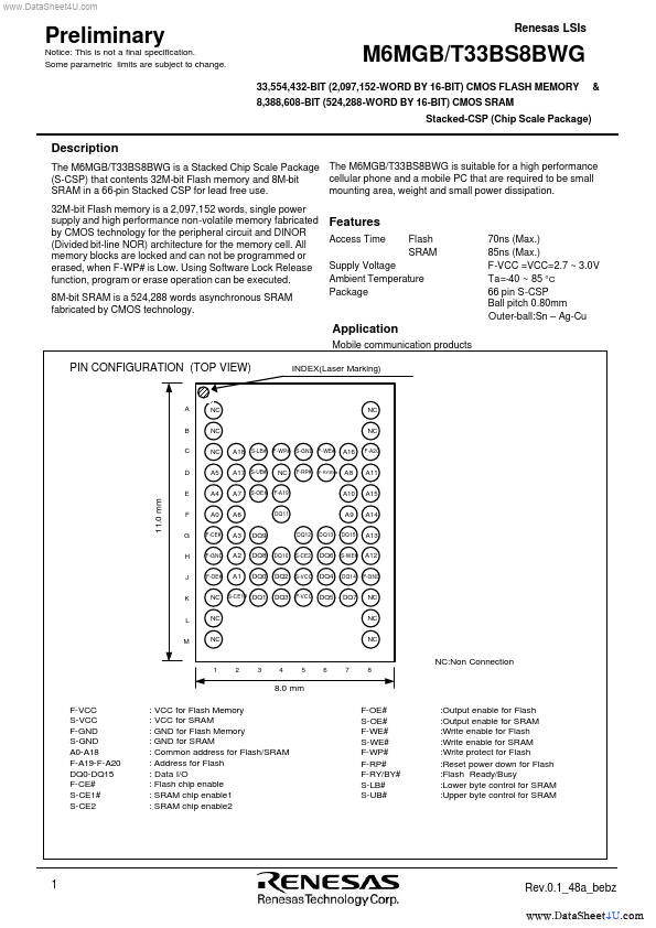
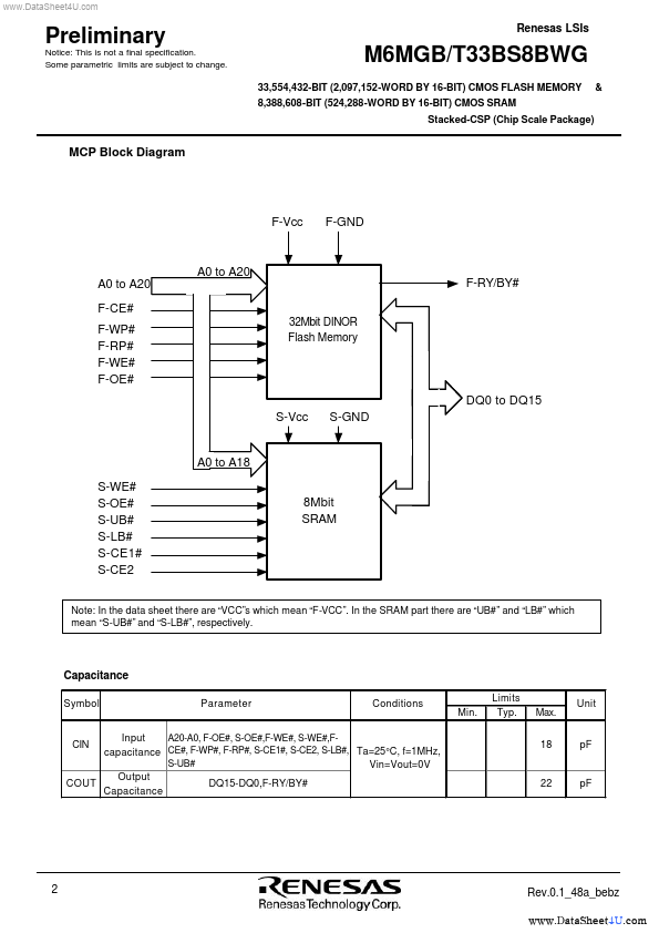
 Description The M6MGB/T33BS8BWG is a Stacked Chip Scale Package The M6MGB/T33BS8BWG is suitable for a high performance cellular phone and a mobile PC that are required to be small (S-CSP) that contents 32M-bit Flash memory and 8M-bit mounting area, weight and small power dissipation. SRAM in a 66-pin Stacked CSP for lead free use.
Published: |